- 您現(xiàn)在的位置:買賣IC網(wǎng) > PDF目錄361035 > LM9811 (National Semiconductor Corporation) 10-Bit Greyscale/30-Bit Color Linear CCD Sensor Processor PDF資料下載
參數(shù)資料
| 型號: | LM9811 |
| 廠商: | National Semiconductor Corporation |
| 英文描述: | 10-Bit Greyscale/30-Bit Color Linear CCD Sensor Processor |
| 中文描述: | 10位Greyscale/30-Bit彩色線陣CCD傳感器處理器 |
| 文件頁數(shù): | 6/36頁 |
| 文件大?。?/td> | 605K |
| 代理商: | LM9811 |
第1頁第2頁第3頁第4頁第5頁當(dāng)前第6頁第7頁第8頁第9頁第10頁第11頁第12頁第13頁第14頁第15頁第16頁第17頁第18頁第19頁第20頁第21頁第22頁第23頁第24頁第25頁第26頁第27頁第28頁第29頁第30頁第31頁第32頁第33頁第34頁第35頁第36頁
AC Electrical Characteristics, MCLK Dependent
(Continued)
The following specifications apply for AGND = DGND = DGND
= 0V, V
= V
= V
= +5.0V
, REF IN = +1.225V
DC
,
f
= 20MHz, t
= 1/f
, t
= t
f
= 5ns, R
= 25
, C
(databus loading) = 50 pF/pin. Refer to Table 2
. Configuration
Register Parameters
for limits labelled
C.R. Boldface limits apply for T
A
= T
J
= T
MIN
to T
MAX
; all other limits T
A
= T
J
=
25C.
Symbol
Parameter
Conditions
Typical
(Note 9)
Limits
(Note 10)
Units
(Limits)
t
S/HREF
Falling Edge of
φ
1 to Ref. Sample
Either Edge of
φ
1 to Ref. Sample
Falling Edge of
φ
1 to Sig. Sample
Either Edge of
φ
1 to Sig. Sample
Sample Pulse Width
(Acquisition Time)
SYNC Low Between Lines
SYNC Setup of
φ
1 to End Line
CCLK Pulse Width
Data Valid Time from EOC Low
EOC Pulse Width
Standard CCD Mode
Even/Odd CCD Mode
Standard CCD Mode
Even/Odd CCD Mode
C.R.
ns
t
S/HSIG
C.R.
ns
t
S/HWIDTH
50ns
1
t
MCLK
t
SYNCLOW
t
B
t
CCLKWIDTH
t
DATAVALID
t
EOCWIDTH
100ns
2
2
5
t
MCLK
(min)
t
MCLK
(max)
t
MCLK
ns (min)
t
MCLK
Hz
Hz
%
250ns
300
5
f
MCLK
/
8
f
MCLK
/
16
50
250ns
2.5MHz
1.25MHz
φ
1 and
φ
2 Frequency
Standard CCD Mode
Even/Odd CCD Mode
φ
1 and
φ
2 Duty Cycle
Electrical Characteristics (Notes)
Note 1:
Absolute Maximum Ratings indicate limits beyond which damage to the device may occur. Operating Ratings indicate conditions for which the device is
functional, but do not guarantee specific performance limits. For guaranteed specifications and test conditions, see the Electrical Characteristics. The guaranteed
specifications apply only for the test conditions listed. Some performance characteristics may degrade when the device is not operated under the listed test condi-
tions.
Note 2:
All voltages are measured with respect to GND = AGND = DGND = DGND
(I/O)
= 0V, unless otherwise specified.
Note 3:
When the input voltage (V
) at any pin exceeds the power supplies (V
<
GND or V
>
V
or V
), the current at that pin should be limited to 25 mA.
The 50 mA maximum package input current rating limits the number of pins that can simultaneously safely exceed the power supplies with an input current of 25
mA to two.
Note 4:
The maximum power dissipation must be derated at elevated temperatures and is dictated by T
,
θ
and the ambient temperature, T
. The maximum
allowable power dissipation at any temperature is P
= (T
–T
)/
θ
. T
= 150C for this device. The typical thermal resistance (
θ
JA
) of this part when board
mounted is 52C/W for the V52A PLCC package, and 70C/W for the VEG52A TQFP package.
Note 5:
Human body model, 100pF capacitor discharged through a 1.5 k
resistor.
Note 6:
See AN450 “Surface Mounting Methods and Their Effect on Product Reliability” or the section titled “Surface Mount” found in any National Semiconductor
Linear Data Book for other methods of soldering surface mount devices.
Note 7:
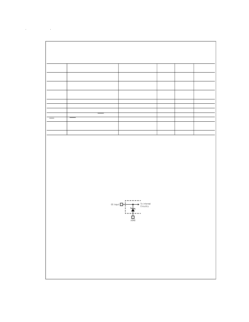
A Zener diode clamps the OS analog input to AGND as shown below. This input protection, in combination with the external clamp capacitor and the output
impedance of the CCD, prevents damage to the LM9811 from transients during power-up.
Note 8:
To guarantee accuracy, it is required that V
A
and V
D
be connected together to the same power supply with separate bypass capacitors at each supply pin.
Note 9:
Typicals are at T
J
= T
A
= 25C, f
MCLK
= 20MHz, and represent most likely parametric norm.
Note 10:
Tested limits are guaranteed to National’s AOQL (Average Outgoing Quality Level).
DS012813-4
www.national.com
6
相關(guān)PDF資料 |
PDF描述 |
|---|---|
| LM9811CCV | 10-Bit Greyscale/30-Bit Color Linear CCD Sensor Processor |
| LM9831CCVJD | LM9831 42-Bit Color, 1200dpi USB Image Scanner |
| LM9831 | LM9831 42-Bit Color, 1200dpi USB Image Scanner |
| LM9831CCVJDX | LM9831 42-Bit Color, 1200dpi USB Image Scanner |
| LM9832CCVJD | LM9832 42-Bit Color, 1200dpi USB Image Scanner |
相關(guān)代理商/技術(shù)參數(shù) |
參數(shù)描述 |
|---|---|
| LM9811CCV | 制造商:NSC 制造商全稱:National Semiconductor 功能描述:10-Bit Greyscale/30-Bit Color Linear CCD Sensor Processor |
| LM9811CCVF | 制造商:NSC 制造商全稱:National Semiconductor 功能描述:10-Bit Greyscale/30-Bit Color Linear CCD Sensor Processor |
| LM9812 | 制造商:NSC 制造商全稱:National Semiconductor 功能描述:LM9812 30-Bit Color Linear CCD Sensor Processor |
| LM9812CCV | 制造商:NSC 制造商全稱:National Semiconductor 功能描述:LM9812 30-Bit Color Linear CCD Sensor Processor |
| LM981-SC36 | 功能描述:基本/快動開關(guān) Foot Switch RoHS:否 制造商:Omron Electronics 觸點形式:SPDT 執(zhí)行器:Lever 電流額定值:5 A 電壓額定值 AC:250 V 電壓額定值 DC:30 V 功率額定值: 工作力:120 g IP 等級:IP 67 NEMA 額定值: 端接類型:Wire 安裝:Panel |
發(fā)布緊急采購,3分鐘左右您將得到回復(fù)。