- 您現(xiàn)在的位置:買賣IC網(wǎng) > PDF目錄358790 > LH28F020SU-L (Sharp Corporation) 2M (256K 】 8) Flash Memory PDF資料下載
參數(shù)資料
| 型號: | LH28F020SU-L |
| 廠商: | Sharp Corporation |
| 英文描述: | 2M (256K 】 8) Flash Memory |
| 中文描述: | 200萬(256K】8)閃存 |
| 文件頁數(shù): | 7/31頁 |
| 文件大小: | 245K |
| 代理商: | LH28F020SU-L |
第1頁第2頁第3頁第4頁第5頁第6頁當(dāng)前第7頁第8頁第9頁第10頁第11頁第12頁第13頁第14頁第15頁第16頁第17頁第18頁第19頁第20頁第21頁第22頁第23頁第24頁第25頁第26頁第27頁第28頁第29頁第30頁第31頁

2M (256K × 8) Flash Memory
LH28F020SU-L
7
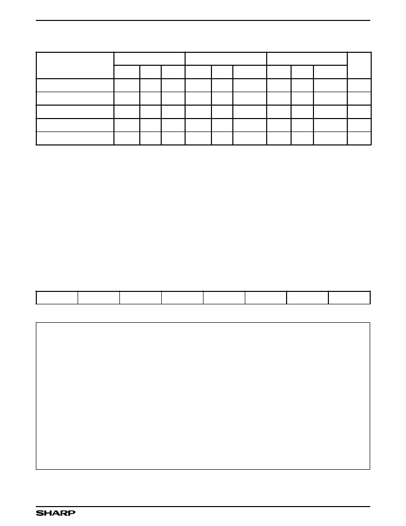
LH28F020SU-L Performance Enhancement Command Bus Definitions
ADDRESS
BA = Block Address
WA = Write Address
X = Don’t Care
DATA
AD = Array Data
WD (L, H) = Write Data (Low, High)
WD (H, L) = Write Data (High, Low)
NOTES:
1. After initial device power-up, or chip reset is completed, the clock lock status bits default to the locked state independent of the data in
the corresponding lock bits. In order to upload the lock bit status, it requires to write Protect Set/Confirm command.
2. To reflect the actual lock-bit status, the Protect Set/Confirm command must be written after Lock Block/Confirm command.
3. When Protect Reset/Confirm command is written, all blocks can be written and erased regardless of the state of the lock-bits.
4. The Lock Block/Confirm command must be written after Protect Reset/Confirm command was written.
5. A
0
is automatically complemented to load second byte of data A
0
value determines which WD is supplied first: A
0
= 0 looks at the
WDL, A
0
= 1 looks at the WDH.
6. Second bus cycle address of Protect Set/Confirm and Protect Reset/Confirm command is 0FFH. Specifically A
9
- A
8
= 0, A
7
- A
0
= 1,
others are don’t care.
COMMAND
FIRST BUS CYCLE
SECOND BUS CYCLE
THIRD BUS CYCLE
NOTE
OPER.
ADD.
DATA
OPER.
ADD.
DATA
OPER.
ADD.
DATA
Protect Set/Confirm
Write
X
57H
Write
0FFH
D0H
1, 2, 6
Protect Reset/Confirm
Write
X
47H
Write
0FFH
D0H
3, 6
Lock Block/Confirm
Write
X
77H
Write
BA
D0H
1, 2, 4
Erase All Unlocked Blocks
Write
X
A7H
Write
X
D0H
1, 2
Two-Byte Write
Write
X
FBH
Write
A0
WD (L, H)
Write
WA
WD (H, L) 1, 2, 5
WSMS
ESS
ES
DWS
VPPS
R
R
R
7
6
5
4
3
2
1
0
Compatible Status Register
CSR.7 = WRITE STATE MACHINE STATUS (WSMS)
1 = Ready
0 = Busy
CSR.6 = ERASE-SUSPEND STATUS (ESS)
1 = Erase Suspended
0 = Erase in Progress/Completed
CSR.5 = ERASE STATUS (ES)
1 = Error in Block Erasure
0 = Successful Block Erase
CSR.4 = DATA-WRITE STATUS (DWS)
1 = Error in Data Write
0 = Data Write Successful
CSR.3 = V
PP
STATUS (VPPS)
1 = V
PP
Low Detect, Operation Abort
0 = V
PP
OK
NOTES:
1. WSMS bit must be checked to determine completion of
an operation (Erase Suspend, Erase or Data Write) before
the appropriate Status bit (ESS, ES or DWS) is checked for
success.
2. If DWS and ES are set to ‘1’ during an erase attempt, an
improper command sequence was entered. Clear the CSR
and attempt the operation again.
3. The VPPS bit, unlike an A/D converter, does not provide
continuous indication of V
PP
level. The WSM interrogates
V
PP
’s level only after the Data-Write or Erase command
sequences have been entered, and informs the system if
V
PP
has not been switched on. VPPS is not guaranteed to
report accurate feedback between V
PPL
and V
PPH
.
相關(guān)PDF資料 |
PDF描述 |
|---|---|
| LH28F020SU-N | 2M (256K 】 8) Flash Memory |
| LH28F040SUTD-Z4 | 4M (512K 】 8) Flash Memory |
| LH28F160BHE-TTL90 | 16M (x8/x16) Flash Memory |
| LH28F160BJE-BTL90 | 16M-BIT(1Mbit x16/2Mbit x8)Boot Block Flash MEMORY(16M位(1M位 x16/2M位 x8)Boot Block 閃速存儲器) |
| LH28F160BJE-TTL70 | 16M-BIT(1Mbit x16/2Mbit x8)Boot Block Flash MEMORY(16M位(1M位 x16/2M位 x8)Boot Block 閃速存儲器) |
相關(guān)代理商/技術(shù)參數(shù) |
參數(shù)描述 |
|---|---|
| LH28F020SU-N | 制造商:SHARP 制造商全稱:Sharp Electrionic Components 功能描述:2M (256K 】 8) Flash Memory |
| LH28F020SUN-L12 | 制造商:未知廠家 制造商全稱:未知廠家 功能描述:x8 Flash EEPROM |
| LH28F032SUTD-70 | 制造商:未知廠家 制造商全稱:未知廠家 功能描述:x8/x16 Flash EEPROM Module |
| LH28F040SUTD-Z4 | 制造商:SHARP 制造商全稱:Sharp Electrionic Components 功能描述:4M (512K 】 8) Flash Memory |
| LH28F0I6SCT-L95 | 制造商:Sharp Microelectronics Corporation 功能描述: |
發(fā)布緊急采購,3分鐘左右您將得到回復(fù)。