- 您現(xiàn)在的位置:買賣IC網 > PDF目錄30729 > LC07410LG SPECIALTY CONSUMER CIRCUIT, PBGA40 PDF資料下載
參數(shù)資料
| 型號: | LC07410LG |
| 元件分類: | 消費家電 |
| 英文描述: | SPECIALTY CONSUMER CIRCUIT, PBGA40 |
| 封裝: | 4.40 X 3.60 MM, FLGA-40 |
| 文件頁數(shù): | 5/36頁 |
| 文件大小: | 367K |
| 代理商: | LC07410LG |
第1頁第2頁第3頁第4頁當前第5頁第6頁第7頁第8頁第9頁第10頁第11頁第12頁第13頁第14頁第15頁第16頁第17頁第18頁第19頁第20頁第21頁第22頁第23頁第24頁第25頁第26頁第27頁第28頁第29頁第30頁第31頁第32頁第33頁第34頁第35頁第36頁
LC07410LG
No.A1345-13/36
Specification Details
Power down/system reset
When the PDNB pin is set to 0, all the circuits are set to power down mode regardless of the power down settings for
each block. A 0 on the PDNB pin also triggers a system reset.
After the power is first applied, the system must be reset without fail.
[See the section on “Checkpoint_2) Resetting”]
After resetting, the contents of the serial port register are initialized.
The VREF buffer is activated by releasing power down mode by setting the PDNB pin from 0 to 1, and then by setting
VREF_BIAS[1:0] to 01. When VREF_BIAS [1:0] is set to 10, VREF starts. Along with the start of VREF, the LINE
output pin is biased to 1/2VDDA. Once the VREF voltage has stabilized, VREF_BIAS [1:0] must be set to 11 (normal
state).
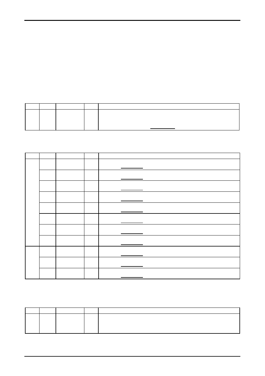
Reference voltage generator circuit
VREF_BIAS: Voltage Reference Bias
* Bold letters indicate initial settings.
ADRS
Bit
Name
Init
Description
01h
[5:4]
VREF_BIAS
00b
Sets the reference voltage circuit (VREF pin).
11: Normal operation (standard resistor value)
10: Quick rise to reference voltage <*1>
01: Activates IREF bias, VREF OFF 00: Power down
<*1> The target voltage is reached quickly by connecting a low-resistance element in the “reference voltage generation
circuit.” During normal operation, a standard resistance is recommended in order to save power.
Power Control
ADRS
Bit
Name
Init
Description
[7]
MIC_PDX
0b
MIC amplifier circuit, power control
1: power on
0: power down
[6]
MIC_PWR_PDX
0b
MIC power circuit (MIC_PWR pin), power control
1: power on
0: power down
[5]
PGA_PDX
0b
PGA circuit, power control
1: power on
0: power down
[4]
ADC_PDX
0b
ADC circuit, power control
1: power on
0: power down
[3]
DAC_PDX
0b
DAC circuit, power control
1: power on
0: power down
[2]
SEL_PDX
0b
Selector (LOUT2) circuit, power control
1: power on
0: power down
[1]
LO_PDX
0b
Line out circuit (LOUT1) circuit, power control
1: power on
0: power down
00h
[0]
SP_PDX
0b
Speaker amplifier circuit, power control
1: power on
0: power down
[2]
PLL_PDX
0b
PLL circuit, power control
1: power on
0: power down (PLL-EXT mode)
[1]
REG_PDX
0b
Regulator circuit, power control
1: power on
0: power down
01h
[0]
VD_PDX
0b
Video driver circuit, power control
1: power on
0: power down
Sampling Frequency Setting
Set sampling frequency used by FS [4:0] register. This is necessary to make it for correctly setting digital frequency
characteristic and ALC damping time constant. The setting is adjusted to a value that is the closest to fs used.
ADRS
Bit
Name
Init
Description
15h
[3:0]
FS
1000b
Sampling Frequency Setting
1000: 48kHz/0111: 44.1kHz/0110: 32kHz/0101: 24kHz
0100: 22.05kHz/0011: 16kHz/0010: 12kHz/0001: 11.025kHz
0000: 8kHz
Note: This setting doesn’t synchronize with PLL setting. It is necessary to set it individually respectively.
Refer to the page of PLL function explanation for PLL setting.
相關PDF資料 |
PDF描述 |
|---|---|
| LC07410LG | SPECIALTY CONSUMER CIRCUIT, PBGA40 |
| LC074146LP | 1 CHANNEL, AUDIO/VIDEO AMPLIFIER, QCC40 |
| LC074146LP | 1 CHANNEL, AUDIO/VIDEO AMPLIFIER, QCC40 |
| LC19001A010 | SPECIALTY CONSUMER CIRCUIT, PQFP80 |
| LC403--CDC | SPECIALTY CONSUMER CIRCUIT, PDIP16 |
相關代理商/技術參數(shù) |
參數(shù)描述 |
|---|---|
| LC074146LP | 制造商:SANYO 制造商全稱:Sanyo Semicon Device 功能描述:CMOS IC Monaural CODEC+Audio I/F +Video driver IC |
| LC07422T | 制造商:SANYO 制造商全稱:Sanyo Semicon Device 功能描述:CMOS IC Audio CODEC with Video Driver |
| LC07424LP | 制造商:SANYO 制造商全稱:Sanyo Semicon Device 功能描述:CMOS IC Audio CODEC with Video Driver |
| LC07424LP-MPB-E | 功能描述:接口—CODEC RoHS:否 制造商:Texas Instruments 類型: 分辨率: 轉換速率:48 kSPs 接口類型:I2C ADC 數(shù)量:2 DAC 數(shù)量:4 工作電源電壓:1.8 V, 2.1 V, 2.3 V to 5.5 V 最大工作溫度:+ 85 C 安裝風格:SMD/SMT 封裝 / 箱體:DSBGA-81 封裝:Reel |
| LC08000E-2H | 制造商:ON Semiconductor 功能描述:MOTOR VECTOR CONTROL IC - Trays 制造商:ON Semiconductor 功能描述:FTRAY / MOTOR VECTOR CONTROL IC |
發(fā)布緊急采購,3分鐘左右您將得到回復。