- 您現(xiàn)在的位置:買賣IC網(wǎng) > PDF目錄383237 > L6563 (意法半導(dǎo)體) ADVANCED TRANSITION-MODE PFC CONTROLLER PDF資料下載
參數(shù)資料
| 型號: | L6563 |
| 廠商: | 意法半導(dǎo)體 |
| 元件分類: | 基準(zhǔn)電壓源/電流源 |
| 英文描述: | ADVANCED TRANSITION-MODE PFC CONTROLLER |
| 中文描述: | 先進(jìn)的轉(zhuǎn)型模式PFC控制器 |
| 文件頁數(shù): | 14/25頁 |
| 文件大?。?/td> | 362K |
| 代理商: | L6563 |
L6563
14/25
In this way a change of the line voltage will cause an inversely proportional change of the half sine ampli-
tude at the output of the multiplier (if the line voltage doubles the amplitude of the multiplier output will be
halved and vice versa) so that the current reference is adapted to the new operating conditions with (ide-
ally) no need for invoking the slow dynamics of the error amplifier. Additionally, the loop gain will be con-
stant throughout the input voltage range, which improves significantly dynamic behavior at low line and
simplifies loop design.
Actually, deriving a voltage proportional to the RMS line voltage implies a form of integration, which has
its own time constant. If it is too small the voltage generated will be affected by a considerable amount of
ripple at twice the mains frequency that will cause distortion of the current reference (resulting in high THD
and poor PF); if it is too large there will be a considerable delay in setting the right amount of feedforward,
resulting in excessive overshoot and undershoot of the pre-regulator's output voltage in response to large
line voltage changes. Clearly a trade-off is required.
The L6563 realizes Voltage Feedforward with a technique that makes use of just two external parts and
that limits the feedforward time constant trade-off issue to only one direction. A capacitor C
FF
and a resis-
tor R
FF
, both connected from the VFF (#5) pin to ground, complete an internal peak-holding circuit that
provides a DC voltage equal to the peak of the rectified sine wave applied on pin MULT (#3). R
FF
provides
a means to discharge C
FF
when the line voltage decreases (see
Figure 36
). In this way, in case of sudden
line voltage rise, C
FF
will be rapidly charged through the low impedance of the internal diode and no ap-
preciable overshoot will be visible at the pre-regulator's output; in case of line voltage drop C
FF
will be dis-
charged with the time constant R
FF
·C
FF
, which can be in the hundred ms to achieve an acceptably low
steady-state ripple and have low current distortion; consequently the output voltage can experience a con-
siderable undershoot, like in systems with no feedforward compensation.
The twice-mains-frequency (2·f
L
) ripple appearing across C
FF
is triangular with a peak-to-peak amplitude
that, with good approximation, is given by:
,
where f
L
is the line frequency. The amount of 3
rd
harmonic distortion introduced by this ripple, related to
the amplitude of its 2·f
L
component, will be:
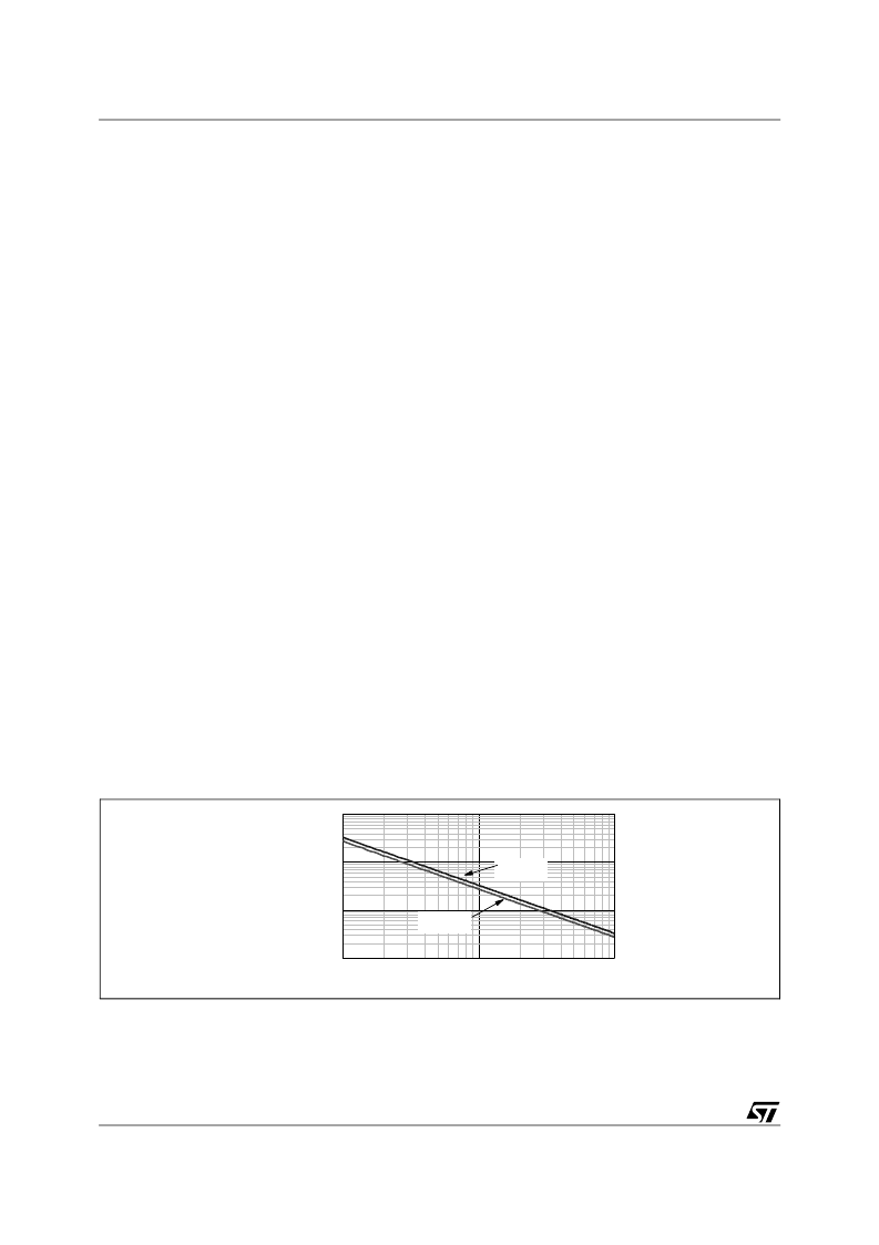
Figure 37
shows a diagram that helps choose the time constant R
FF
·C
FF
based on the amount of maxi-
mum desired 3
rd
harmonic distortion. Always connect R
FF
and C
FF
to the pin, the IC will not work properly
if the pin is either left floating or connected directly to ground.
Figure 37. R
FF
·C
FF
as a function of 3
rd
harmonic distortion introduced in the input current
The dynamics of the voltage feedforward input is limited downwards at 0.5V (see
Figure 36
), that is the
output of the multiplier will not increase any more if the voltage on the V
FF
pin is below 0.5V. This helps to
prevent excessive power flow when the line voltage is lower than the minimum specified value
V
FF
2V
4f
L
R
FF
C
FF
+
1
----------------------------------------
=
D
3
%
2
π
f
L
R
FF
C
FF
----------------------------------
=
D %
0.1
1
10
0.01
0.1
1
10
f = 50 Hz
f = 60 Hz
R · C [s]
相關(guān)PDF資料 |
PDF描述 |
|---|---|
| L6563TR | ADVANCED TRANSITION-MODE PFC CONTROLLER |
| L6566A | Multi-mode controller for SMPS with PFC front-end |
| L6566ATR | Multi-mode controller for SMPS with PFC front-end |
| L6566B | Multi-mode controller for SMPS |
| L6566BTR | Multi-mode controller for SMPS |
相關(guān)代理商/技術(shù)參數(shù) |
參數(shù)描述 |
|---|---|
| L6563_07 | 制造商:STMICROELECTRONICS 制造商全稱:STMicroelectronics 功能描述:Advanced transition-mode PFC controller |
| L6563A | 功能描述:功率因數(shù)校正 IC Advanced transition mode PFC controller RoHS:否 制造商:Fairchild Semiconductor 開關(guān)頻率:300 KHz 最大功率耗散: 最大工作溫度:+ 125 C 安裝風(fēng)格:SMD/SMT 封裝 / 箱體:SOIC-8 封裝:Reel |
| L6563ATR | 功能描述:功率因數(shù)校正 IC Advanced transition mode PFC controller RoHS:否 制造商:Fairchild Semiconductor 開關(guān)頻率:300 KHz 最大功率耗散: 最大工作溫度:+ 125 C 安裝風(fēng)格:SMD/SMT 封裝 / 箱體:SOIC-8 封裝:Reel |
| L6563CYTR | 制造商:ST 功能描述:ADVANCED TRANSITION-MODE PFC CONTROLLER |
| L6563H | 功能描述:功率因數(shù)校正 IC High voltage start Transition-mode PFC RoHS:否 制造商:Fairchild Semiconductor 開關(guān)頻率:300 KHz 最大功率耗散: 最大工作溫度:+ 125 C 安裝風(fēng)格:SMD/SMT 封裝 / 箱體:SOIC-8 封裝:Reel |
發(fā)布緊急采購,3分鐘左右您將得到回復(fù)。