- 您現(xiàn)在的位置:買賣IC網(wǎng) > PDF目錄383237 > L6563 (意法半導(dǎo)體) ADVANCED TRANSITION-MODE PFC CONTROLLER PDF資料下載
參數(shù)資料
| 型號(hào): | L6563 |
| 廠商: | 意法半導(dǎo)體 |
| 元件分類: | 基準(zhǔn)電壓源/電流源 |
| 英文描述: | ADVANCED TRANSITION-MODE PFC CONTROLLER |
| 中文描述: | 先進(jìn)的轉(zhuǎn)型模式PFC控制器 |
| 文件頁(yè)數(shù): | 12/25頁(yè) |
| 文件大小: | 362K |
| 代理商: | L6563 |
第1頁(yè)第2頁(yè)第3頁(yè)第4頁(yè)第5頁(yè)第6頁(yè)第7頁(yè)第8頁(yè)第9頁(yè)第10頁(yè)第11頁(yè)當(dāng)前第12頁(yè)第13頁(yè)第14頁(yè)第15頁(yè)第16頁(yè)第17頁(yè)第18頁(yè)第19頁(yè)第20頁(yè)第21頁(yè)第22頁(yè)第23頁(yè)第24頁(yè)第25頁(yè)
L6563
12/25
4
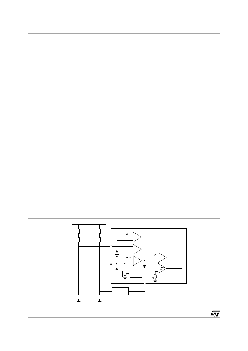
APPLICATION INFORMATION
4.1 Overvoltage protection
Normally, the voltage control loop keeps the output voltage Vo of the PFC pre-regulator close to its nominal
value, set by the ratio of the resistors R1 and R2 of the output divider. Neglecting the ripple components,
under steady state conditions the current through R1 equals that through R2. Considering that the non-in-
verting input of the error amplifier is internally biased at 2.5V, the voltage at pin INV will be 2.5V as well, then:
R2
.
If the output voltage experiences an abrupt change
Vo the voltage at pin INV is kept at 2.5V by the local
feedback of the error amplifier, a network connected between pins INV and COMP that introduces a long
time constant. Then the current through R2 remains equal to 2.5/R2 but that through R1 becomes:
V
–
------------------------+
=
.
The difference current
I
R1
= I’
R1
- I’
R1
=
V
O
/R1 will flow through the compensation network and enter the
error amplifier (pin COMP). This current is monitored inside the IC and when it reaches about 18 μA the out-
put voltage of the multiplier is forced to decrease, thus reducing the energy drawn from the mains. If the cur-
rent exceeds 20 μA, the OVP is triggered (Dynamic OVP), and the external power transistor is switched off
until the current falls approximately below 5 μA. However, if the overvoltage persists (e.g. in case the load
is completely disconnected), the error amplifier will eventually saturate low hence triggering an internal com-
parator (Static OVP) that will keep the external power switch turned off until the output voltage comes back
close to the regulated value. The output overvoltage that is able to trigger the OVP function is then:
V
O
= R1 · 20 · 10
-6
An important advantage of this technique is that the overvoltage level can be set independently of the reg-
ulated output voltage: the latter depends on the ratio of R1 to R2, the former on the individual value of R1.
Another advantage is the precision: the tolerance of the detection current is 15%, which means 15% tol-
erance on the
Vo. Since it is usually much smaller than Vo, the tolerance on the absolute value will be
proportionally reduced.
Example: Vo=400V,
Vo=40V. Then: R1=40V/20μA=2M
; R2=2.5·2M
·/(400-2.5)=12.58k
. The toler-
ance on the OVP level due to the L6563 will be 40·0.15=6 V, that is ±1.36%.
When either OVP is activated the quiescent consumption is reduced to minimize the discharge of the Vcc
capacitor.
Figure 35. Output voltage setting, OVP and FFP functions: internal block diagram
I
R2
I
R1
-------
V
---------------------
2.5
–
R1
=
=
=
I
'
R1
2.5
R1
O
-
+
2.5V
L6563
1
2
INV
COMP
E/A
-
+
Frequency
Compensation
+
-
R2
7
PFC_OK
I
TBO
-
+
2.25V
Static OVP
-
+
Dynamic OVP
20 μA
Vout
{
R1a
R1b
R1
9.5V
FAULT (latched)
TBO
FUNCTION
R4
{
R3a
R3b
R3
+
-
FAULT (not latched)
0.26V
9.5V
相關(guān)PDF資料 |
PDF描述 |
|---|---|
| L6563TR | ADVANCED TRANSITION-MODE PFC CONTROLLER |
| L6566A | Multi-mode controller for SMPS with PFC front-end |
| L6566ATR | Multi-mode controller for SMPS with PFC front-end |
| L6566B | Multi-mode controller for SMPS |
| L6566BTR | Multi-mode controller for SMPS |
相關(guān)代理商/技術(shù)參數(shù) |
參數(shù)描述 |
|---|---|
| L6563_07 | 制造商:STMICROELECTRONICS 制造商全稱:STMicroelectronics 功能描述:Advanced transition-mode PFC controller |
| L6563A | 功能描述:功率因數(shù)校正 IC Advanced transition mode PFC controller RoHS:否 制造商:Fairchild Semiconductor 開關(guān)頻率:300 KHz 最大功率耗散: 最大工作溫度:+ 125 C 安裝風(fēng)格:SMD/SMT 封裝 / 箱體:SOIC-8 封裝:Reel |
| L6563ATR | 功能描述:功率因數(shù)校正 IC Advanced transition mode PFC controller RoHS:否 制造商:Fairchild Semiconductor 開關(guān)頻率:300 KHz 最大功率耗散: 最大工作溫度:+ 125 C 安裝風(fēng)格:SMD/SMT 封裝 / 箱體:SOIC-8 封裝:Reel |
| L6563CYTR | 制造商:ST 功能描述:ADVANCED TRANSITION-MODE PFC CONTROLLER |
| L6563H | 功能描述:功率因數(shù)校正 IC High voltage start Transition-mode PFC RoHS:否 制造商:Fairchild Semiconductor 開關(guān)頻率:300 KHz 最大功率耗散: 最大工作溫度:+ 125 C 安裝風(fēng)格:SMD/SMT 封裝 / 箱體:SOIC-8 封裝:Reel |
發(fā)布緊急采購(gòu),3分鐘左右您將得到回復(fù)。