- 您現(xiàn)在的位置:買賣IC網(wǎng) > PDF目錄373155 > KM418RD2AD (SAMSUNG SEMICONDUCTOR CO. LTD.) 128/144Mbit RDRAM 256K x 16/18 bit x 2*16 Dependent Banks Direct RDRAMTM PDF資料下載
參數(shù)資料
| 型號: | KM418RD2AD |
| 廠商: | SAMSUNG SEMICONDUCTOR CO. LTD. |
| 英文描述: | 128/144Mbit RDRAM 256K x 16/18 bit x 2*16 Dependent Banks Direct RDRAMTM |
| 中文描述: | 128/144Mbit RDRAM的256 × 16/18位× 2 * 16屬銀行直接RDRAMTM |
| 文件頁數(shù): | 42/64頁 |
| 文件大小: | 4052K |
| 代理商: | KM418RD2AD |
第1頁第2頁第3頁第4頁第5頁第6頁第7頁第8頁第9頁第10頁第11頁第12頁第13頁第14頁第15頁第16頁第17頁第18頁第19頁第20頁第21頁第22頁第23頁第24頁第25頁第26頁第27頁第28頁第29頁第30頁第31頁第32頁第33頁第34頁第35頁第36頁第37頁第38頁第39頁第40頁第41頁當前第42頁第43頁第44頁第45頁第46頁第47頁第48頁第49頁第50頁第51頁第52頁第53頁第54頁第55頁第56頁第57頁第58頁第59頁第60頁第61頁第62頁第63頁第64頁
Page 39
KM416RD8AC(D)/KM418RD8AC(D)
Direct RDRAM
Rev. 1.01 Oct. 1999
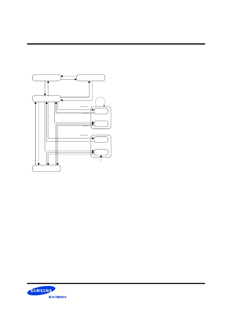
able to frame COL packets (TFRM is a control register field
- see Figure 40). Once in ATTN state, the RDRAM will
automatically transition to the ATTNW and ATTNR states
as it receives WR and RD commands.
Once the RDRAM is in ATTN, ATTNW, or ATTNR states, it
will remain there until it is explicitly returned to the STBY
state with a RLX command. A RLX command may be given
in an ROWR, COLC , or COLX packet (see the left side of
Figure 46). It is usually given after all banks of the RDRAM
have been precharged; if other banks are still activated, then
the RLX command would probably not be given.
If a broadcast ROWA packet or ROWR packet (with the
ATTN command) is received, the RDRAM
’
s power state
doesn
’
t change. If a broadcast ROWR packet with RLXR
command is received, the RDRAM goes to STBY.
Figure 47 shows the NAP entry sequence (left). NAP state is
entered by sending a NAPR command in a ROW packet. A
time t
ASN
is required to enter NAP state (this specification is
provided for power calculation purposes). The clock on
CTM/CFM must remain stable for a time t
CD
after the
NAPR command.
The RDRAM may be in ATTN or STBY state when the
NAPR command is issued. When NAP state is exited, the
RDRAM will return to the original starting state (ATTN or
STBY). If it is in ATTN state and a RLXR command is spec-
ified with NAPR, then the RDRAM will return to STBY
state when NAP is exited.
Figure 47 also shows the PDN entry sequence (right). PDN
state is entered by sending a PDNR command in a ROW
packet. A time t
ASP
is required to enter PDN state (this spec-
ification is provided for power calculation purposes). The
clock on CTM/CFM must remain stable for a time t
CD
after
the PDNR command.
The RDRAM may be in ATTN or STBY state when the
PDNR command is issued. When PDN state is exited, the
RDRAM will return to the original starting state (ATTN or
STBY). If it is in ATTN state and a RLXR command is spec-
ified with PDNR, then the RDRAM will return to STBY
state when PDN is exited. The current- and slew-rate-control
levels are re-established.
The RDRAM
’
s write buffer must be retired with the appro-
priate COP command before NAP or PDN are entered. Also,
all the RDRAM
’
s banks must be precharged before NAP or
PDN are entered. The exception to this is if NAP is entered
with the NSR bit of the INIT register cleared (disabling self-
refresh in NAP). The commands for relaxing, retiring, and
precharging may be given to the RDRAM as late as the
ROPa0, COPa0, and XOPa0 packets in Figure 47. No broad-
cast packets nor packets directed to the RDRAM entering
Nap or PDN may overlay the quiet window. This window
extends for a time t
NPQ
after the packet with the NAPR or
PDNR command.
Figure 48 shows the NAP and PDN exit sequences. These
sequences are virtually identical; the minor differences will
be highlighted in the following description.
Before NAP or PDN exit, the CTM/CFM clock must be
stable for a time t
CE
. Then, on a falling and rising edge of
SCK, if there is a
“
01
”
on the CMD input, NAP or PDN state
will be exited. Also, on the falling SCK edge the SIO0 input
must be at a 0 for NAP exit and 1 for PDN exit.
If the PSX bit of the INIT register is 0, then a device
PDEV5..0 is specified for NAP or PDN exit on the DQA5..0
pins. This value is driven on the rising SCK edge 0.5 or 1.5
SCK cycles after the original falling edge, depending upon
the value of the DQS bit of the NAPX register. If the PSX bit
of the INIT register is 1, then the RDRAM ignores the
Figure 45: Power State Transition Diagram
automatic
automatic
a
a
a
a
ATTNR
ATTNW
ATTN
STBY
SETR/CLRR
NAP-A
NAPR RLXR
Notation:
SETR/CLRR - SETR/CLRR Reset sequence in SRQ packets
PDNR - PDNR command in ROWR packet
NAPR - NAPR command in ROWR packet
RLXR - RLX command in ROWR packet
RLX - RLX command in ROWR,COLC,COLX packets
SIO0 - SIO0 input value
PDEV.CMD - (PDEV=DEVID)(CMD=01)
ATTN - ROWA packet (non-broadcast) or ROWR packet
(non-broadcast) with ATTN command
t
NLIMIT
NAP
NAP-S
PDEV.CMDSIO0
NAPR RLXR
PDEV.CMDSIO0
PDN-A
PDNR RLXR
PDN
PDN-S
PDEV.CMDSIO0
PDNR RLXR
PDEV.CMDSIO0
N
P
A
R
相關PDF資料 |
PDF描述 |
|---|---|
| KM418RD2C | 128/144Mbit RDRAM 256K x 16/18 bit x 2*16 Dependent Banks Direct RDRAMTM |
| KM418RD2D | 128/144Mbit RDRAM 256K x 16/18 bit x 2*16 Dependent Banks Direct RDRAMTM |
| KM418RD32AC | 128/144Mbit RDRAM 256K x 16/18 bit x 2*16 Dependent Banks Direct RDRAMTM |
| KM418RD32AD | 128/144Mbit RDRAM 256K x 16/18 bit x 2*16 Dependent Banks Direct RDRAMTM |
| KM418RD32C | 128/144Mbit RDRAM 256K x 16/18 bit x 2*16 Dependent Banks Direct RDRAMTM |
相關代理商/技術參數(shù) |
參數(shù)描述 |
|---|---|
| KM418RD2C | 制造商:SAMSUNG 制造商全稱:Samsung semiconductor 功能描述:128/144Mbit RDRAM 256K x 16/18 bit x 2*16 Dependent Banks Direct RDRAMTM |
| KM418RD2D | 制造商:SAMSUNG 制造商全稱:Samsung semiconductor 功能描述:128/144Mbit RDRAM 256K x 16/18 bit x 2*16 Dependent Banks Direct RDRAMTM |
| KM418RD32AC | 制造商:SAMSUNG 制造商全稱:Samsung semiconductor 功能描述:128/144Mbit RDRAM 256K x 16/18 bit x 2*16 Dependent Banks Direct RDRAMTM |
| KM418RD32AD | 制造商:SAMSUNG 制造商全稱:Samsung semiconductor 功能描述:128/144Mbit RDRAM 256K x 16/18 bit x 2*16 Dependent Banks Direct RDRAMTM |
| KM418RD32C | 制造商:SAMSUNG 制造商全稱:Samsung semiconductor 功能描述:128/144Mbit RDRAM 256K x 16/18 bit x 2*16 Dependent Banks Direct RDRAMTM |
發(fā)布緊急采購,3分鐘左右您將得到回復。