- 您現(xiàn)在的位置:買賣IC網(wǎng) > PDF目錄374311 > KBE00G003M (SAMSUNG SEMICONDUCTOR CO. LTD.) NAND 512Mb*2 + Mobile SDRAM 256Mb*2 PDF資料下載
參數(shù)資料
| 型號: | KBE00G003M |
| 廠商: | SAMSUNG SEMICONDUCTOR CO. LTD. |
| 英文描述: | NAND 512Mb*2 + Mobile SDRAM 256Mb*2 |
| 中文描述: | NAND閃存的512Mb * 2移動SDRAM 256Mb的* 2 |
| 文件頁數(shù): | 36/89頁 |
| 文件大?。?/td> | 1238K |
| 代理商: | KBE00G003M |
第1頁第2頁第3頁第4頁第5頁第6頁第7頁第8頁第9頁第10頁第11頁第12頁第13頁第14頁第15頁第16頁第17頁第18頁第19頁第20頁第21頁第22頁第23頁第24頁第25頁第26頁第27頁第28頁第29頁第30頁第31頁第32頁第33頁第34頁第35頁當(dāng)前第36頁第37頁第38頁第39頁第40頁第41頁第42頁第43頁第44頁第45頁第46頁第47頁第48頁第49頁第50頁第51頁第52頁第53頁第54頁第55頁第56頁第57頁第58頁第59頁第60頁第61頁第62頁第63頁第64頁第65頁第66頁第67頁第68頁第69頁第70頁第71頁第72頁第73頁第74頁第75頁第76頁第77頁第78頁第79頁第80頁第81頁第82頁第83頁第84頁第85頁第86頁第87頁第88頁第89頁
KBE00G003M-D411
MCP MEMORY
July 2005
36
Revision 0.1
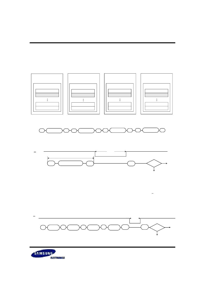
Restirction in addressing with Multi Plane Page Program
While any block in each plane may be addressable for Multi-Plane Page Program, the four least significant addresses(A9-A13) for
the selected pages at one operation must be the same. Figure 13 shows an example where 2nd page of each addressed block is
selected for four planes. However, any arbitrary sequence is allowed in addressing multiple planes as shown in Figure17.
80h
Plane 2
11h
80h
11h
80h
11h
80h
10h
Plane 0
Plane3
Plane 1
Plane 0
(1024 Block)
Plane 1
(1024 Block)
Plane 2
(1024 Block)
Plane 3
(1024 Block)
Page 0
Page 1
Page 31
Page 30
Block 0
Page 0
Page 1
Page 31
Page 30
Block 1
Page 0
Page 1
Page 31
Page 30
Block 2
Page 0
Page 1
Page 31
Page 30
Block 3
Figure 15. Multi-Plane Page Program & Read Status Operation
80h
A
0
~ A
7
& A
9
~ A
26
528 Byte Data
I/O
0
~
7
R/B
Address & Data Input
I/O
Pass
10h
71h
Fail
t
PROG
Last Plane input
Multi-Plane Block Erase into Plane 0~3 or Plane 4~7
Basic concept of Multi-Plane Block Erase operation is identical to that of Multi-Plane Page Program. Up to four blocks, one from each
plane can be simultaneously erased. Standard Block Erase command sequences (Block Erase Setup command followed by three
address cycles) may be repeated up to four times for erasing up to four blocks. Only one block should be selected from each plane.
The Erase Confirm command initiates the actual erasing process. The completion is detected by analyzing R/B pin or Ready/Busy
status (I/O 6). Upon the erase completion, pass/fail status of each block is examined by reading extended pass/fail status(I/O 1
through I/O 4).
Figure 16. Four Block Erase Operation
60h
A
0
~ A
7
& A
9
~ A
26
I/O
0
~
7
R/B
Address
(3 Cycle)
60h
60h
60h
D0h
71h
I/O
Pass
Fail
t
BERS
Address
(3 Cycle)
Address
(3 Cycle)
Address
(3 Cycle)
Figure 13. Multi-Plane Program & Read Status Operation
Figure 14. Addressing Multiple Planes
相關(guān)PDF資料 |
PDF描述 |
|---|---|
| KBE00G003M-D411 | NAND 512Mb*2 + Mobile SDRAM 256Mb*2 |
| KBE00S009M | 1Gb NAND x 2 + 256Mb Mobile SDRAM x 2 |
| KBE00S009M-D411 | 1Gb NAND x 2 + 256Mb Mobile SDRAM x 2 |
| KBJ2501 | 25A SINGLE PHASE SILICON BRIDGE RECTIFIER |
| KBJ2502 | 25A SINGLE PHASE SILICON BRIDGE RECTIFIER |
相關(guān)代理商/技術(shù)參數(shù) |
參數(shù)描述 |
|---|---|
| KBE00G003M-D411 | 制造商:SAMSUNG 制造商全稱:Samsung semiconductor 功能描述:NAND 512Mb*2 + Mobile SDRAM 256Mb*2 |
| KBE00S003M | 制造商:SAMSUNG 制造商全稱:Samsung semiconductor 功能描述:1Gb NAND*2 + 256Mb Mobile SDRAM*2 |
| KBE00S003M-D411 | 制造商:SAMSUNG 制造商全稱:Samsung semiconductor 功能描述:1Gb NAND*2 + 256Mb Mobile SDRAM*2 |
| KBE00S009M | 制造商:SAMSUNG 制造商全稱:Samsung semiconductor 功能描述:1Gb NAND x 2 + 256Mb Mobile SDRAM x 2 |
| KBE00S009M-D411 | 制造商:SAMSUNG 制造商全稱:Samsung semiconductor 功能描述:1Gb NAND x 2 + 256Mb Mobile SDRAM x 2 |
發(fā)布緊急采購,3分鐘左右您將得到回復(fù)。