- 您現(xiàn)在的位置:買賣IC網(wǎng) > PDF目錄9898 > IDT72V2113L7-5PF8 (IDT, Integrated Device Technology Inc)IC FIFO SUPERSYNCII 7-5NS 80TQFP PDF資料下載
參數(shù)資料
| 型號: | IDT72V2113L7-5PF8 |
| 廠商: | IDT, Integrated Device Technology Inc |
| 文件頁數(shù): | 34/46頁 |
| 文件大小: | 0K |
| 描述: | IC FIFO SUPERSYNCII 7-5NS 80TQFP |
| 標準包裝: | 750 |
| 系列: | 72V |
| 功能: | 同步 |
| 存儲容量: | 4.7Mb(262k x 18) |
| 訪問時間: | 5ns |
| 電源電壓: | 3.15 V ~ 3.45 V |
| 工作溫度: | 0°C ~ 70°C |
| 安裝類型: | 表面貼裝 |
| 封裝/外殼: | 80-LQFP |
| 供應商設備封裝: | 80-TQFP(14x14) |
| 包裝: | 帶卷 (TR) |
| 其它名稱: | 72V2113L7-5PF8 |
第1頁第2頁第3頁第4頁第5頁第6頁第7頁第8頁第9頁第10頁第11頁第12頁第13頁第14頁第15頁第16頁第17頁第18頁第19頁第20頁第21頁第22頁第23頁第24頁第25頁第26頁第27頁第28頁第29頁第30頁第31頁第32頁第33頁當前第34頁第35頁第36頁第37頁第38頁第39頁第40頁第41頁第42頁第43頁第44頁第45頁第46頁
4
IDT72V263/273/283/293/103/113 3.3V HIGH DENSITY SUPERSYNC IITM NARROW BUS FIFO
8K x 18, 16K x 9/18, 32K x 9/18, 64K x 9/18, 128K x 9/18, 256K x 9/18, 512K x9
COMMERCIAL AND INDUSTRIAL
TEMPERATURE RANGES
IDT72V2103/72V2113 3.3V HIGH DENSITY SUPERSYNC IITM NARROW BUS FIFO
131,072 x 18/262,144 x 9, 262,144 x 18/524,288 x 9
JUNE 1, 2010
not have to be asserted for accessing the first word. However, subsequent
words written to the FIFO do require a LOW on
REN for access. The state of
the FWFT/SI input during Master Reset determines the timing mode in use.
For applications requiring more data storage capacity than a single FIFO
canprovide,theFWFTtimingmodepermitsdepthexpansionbychainingFIFOs
in series (i.e. the data outputs of one FIFO are connected to the corresponding
data inputs of the next). No external logic is required.
These FIFOs have five flag pins,
EF/OR (Empty Flag or Output Ready),
FF/IR (Full Flag or Input Ready), HF (Half-full Flag), PAE (Programmable
Almost-Emptyflag)and
PAF(ProgrammableAlmost-Fullflag).TheEFandFF
functions are selected in IDT Standard mode. The
IR and OR functions are
selected in FWFT mode.
HF, PAE and PAF are always available for use,
irrespective of timing mode.
PAE and PAFcanbeprogrammedindependentlytoswitchatanypointin
memory.Programmableoffsetsdeterminetheflagswitchingthresholdandcan
beloadedbytwomethods:parallelorserial.Eightdefaultoffsetsettingsarealso
provided, so that
PAEcanbesettoswitchatapredefinednumberoflocations
from the empty boundary and the
PAF threshold can also be set at similar
predefinedvaluesfromthefullboundary.Thedefaultoffsetvaluesaresetduring
Master Reset by the state of the FSEL0, FSEL1, and
LD pins.
Forserialprogramming,
SENtogetherwithLDoneachrisingedgeofWCLK,
are used to load the offset registers via the Serial Input (SI). For parallel
programming,
WEN togetherwithLD oneachrisingedgeofWCLK,areused
to load the offset registers via Dn.
REN together with LD on each rising edge
ofRCLKcanbeusedtoreadtheoffsetsinparallelfromQnregardlessofwhether
serial or parallel offset loading has been selected.
During Master Reset (
MRS)thefollowingeventsoccur:thereadandwrite
pointers are set to the first location of the FIFO. The FWFT pin selects IDT
Standard mode or FWFT mode.
The Partial Reset (
PRS) also sets the read and write pointers to the first
location of the memory. However, the timing mode, programmable flag
programmingmethod,anddefaultorprogrammedoffsetsettingsexistingbefore
PartialResetremainunchanged.Theflagsareupdatedaccordingtothetiming
modeandoffsetsineffect.
PRSisusefulforresettingadeviceinmid-operation,
when reprogramming programmable flags would be undesirable.
Itisalsopossibletoselectthetimingmodeofthe
PAE(ProgrammableAlmost-
Empty flag) and
PAF (Programmable Almost-Full flag) outputs. The timing
modes can be set to be either asynchronous or synchronous for the
PAE and
PAFflags.
If asynchronous
PAE/PAF configuration is selected, the PAE is asserted
LOWontheLOW-to-HIGHtransitionofRCLK.
PAEisresettoHIGHontheLOW-
DESCRIPTION (CONTINUED)
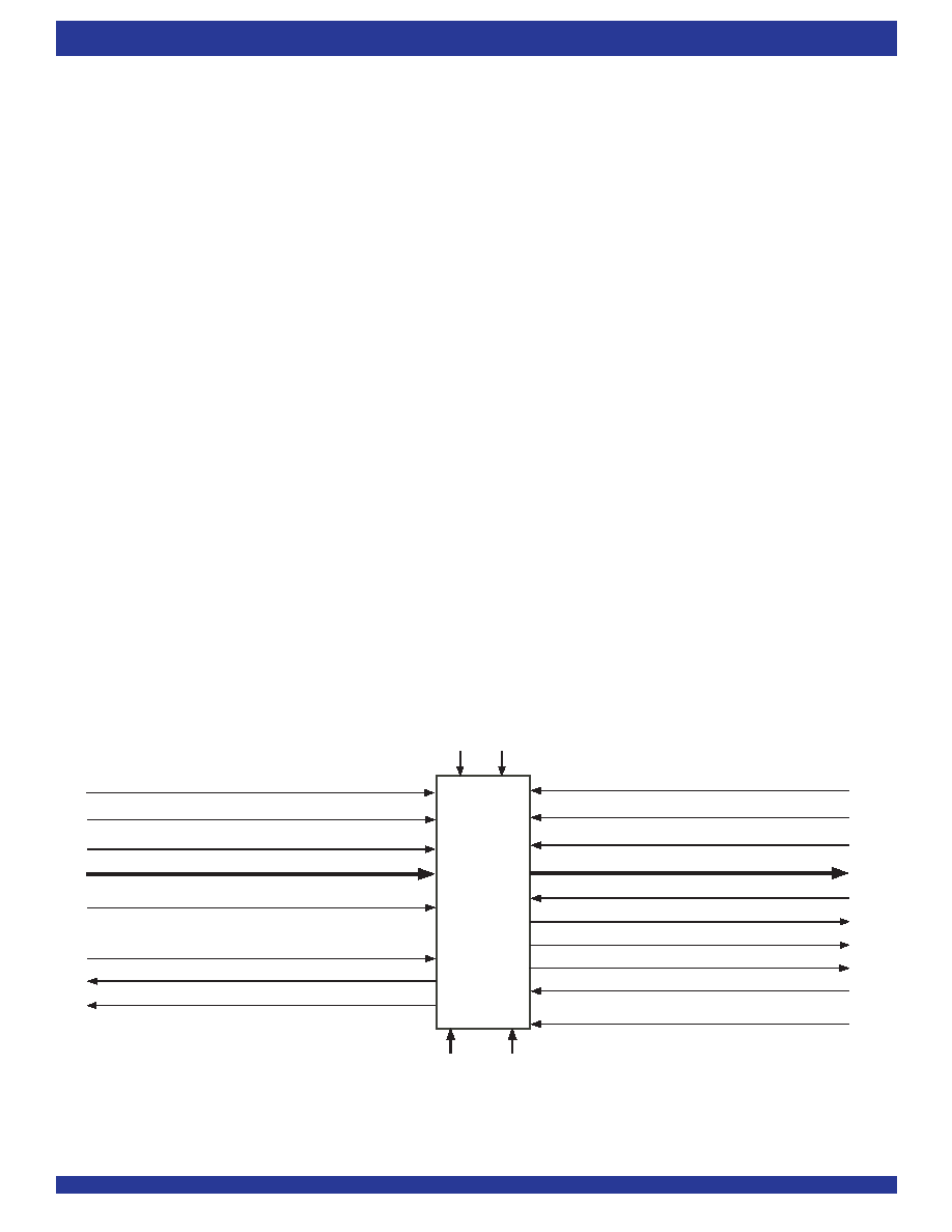
(x9 or x18) DATA OUT (Q0 - Qn)
(x9 or x18) DATA IN (D0 - Dn)
MASTER RESET (MRS)
READ CLOCK (RCLK/RD*)
READ ENABLE (REN)
OUTPUT ENABLE (OE)
EMPTY FLAG/OUTPUT READY (EF/OR)
PROGRAMMABLE ALMOST-EMPTY (PAE)
WRITE CLOCK (WCLK/WR*)
WRITE ENABLE (WEN)
LOAD (LD)
FULL FLAG/INPUT READY (FF/IR)
PROGRAMMABLE ALMOST-FULL (PAF)
IDT
72V2103
72V2113
PARTIAL RESET (PRS)
FIRST WORD FALL THROUGH/SERIAL
INPUT (FWFT/SI)
RETRANSMIT (RT)
6119 drw03
HALF-FULL FLAG (HF)
SERIAL ENABLE(SEN)
INPUT WIDTH
(IW)
OUTPUT WIDTH
(OW)
BIG-ENDIAN/LITTLE-ENDIAN (BE)
INTERSPERSED/
NON-INTERSPERSED PARITY (IP)
Figure 1. Single Device Configuration Signal Flow Diagram
相關PDF資料 |
PDF描述 |
|---|---|
| MS27467E25F61PB | CONN PLUG 61POS STRAIGHT W/PINS |
| IDT72V2113L10PFI8 | IC FIFO SUPERSYNCII 10NS 80-TQFP |
| MAX1416EWE+ | IC ADC 16BIT DELTA SIGMA 16-SOIC |
| IDT72T36105L5BB | IC FIFO 131X18 5NS 240BGA |
| MAX111ACAP+T | IC ADC 14BIT 2CH 5V 20-SSOP |
相關代理商/技術參數(shù) |
參數(shù)描述 |
|---|---|
| IDT72V2113L7-5PFGI | 制造商:Integrated Device Technology Inc 功能描述:IC FIFO SUPERSYNCII 6NS 80TQFP |
| IDT72V211L10J | 功能描述:IC FIFO SYNC 512X9 10NS 32-PLCC RoHS:否 類別:集成電路 (IC) >> 邏輯 - FIFO 系列:72V 標準包裝:80 系列:7200 功能:同步 存儲容量:18.4K(1K x 18) 數(shù)據(jù)速率:- 訪問時間:10ns 電源電壓:4.5 V ~ 5.5 V 工作溫度:0°C ~ 70°C 安裝類型:表面貼裝 封裝/外殼:64-LQFP 供應商設備封裝:64-TQFP(10x10) 包裝:托盤 其它名稱:72225LB10TF |
| IDT72V211L10J8 | 功能描述:IC FIFO SYNC 512X9 10NS 32-PLCC RoHS:否 類別:集成電路 (IC) >> 邏輯 - FIFO 系列:72V 標準包裝:80 系列:7200 功能:同步 存儲容量:18.4K(1K x 18) 數(shù)據(jù)速率:- 訪問時間:10ns 電源電壓:4.5 V ~ 5.5 V 工作溫度:0°C ~ 70°C 安裝類型:表面貼裝 封裝/外殼:64-LQFP 供應商設備封裝:64-TQFP(10x10) 包裝:托盤 其它名稱:72225LB10TF |
| IDT72V211L10PF | 功能描述:IC FIFO SYNC 512X9 10NS 32-TQFP RoHS:否 類別:集成電路 (IC) >> 邏輯 - FIFO 系列:72V 標準包裝:80 系列:7200 功能:同步 存儲容量:18.4K(1K x 18) 數(shù)據(jù)速率:- 訪問時間:10ns 電源電壓:4.5 V ~ 5.5 V 工作溫度:0°C ~ 70°C 安裝類型:表面貼裝 封裝/外殼:64-LQFP 供應商設備封裝:64-TQFP(10x10) 包裝:托盤 其它名稱:72225LB10TF |
| IDT72V211L10PF8 | 功能描述:IC FIFO SYNC 512X9 10NS 32-TQFP RoHS:否 類別:集成電路 (IC) >> 邏輯 - FIFO 系列:72V 標準包裝:80 系列:7200 功能:同步 存儲容量:18.4K(1K x 18) 數(shù)據(jù)速率:- 訪問時間:10ns 電源電壓:4.5 V ~ 5.5 V 工作溫度:0°C ~ 70°C 安裝類型:表面貼裝 封裝/外殼:64-LQFP 供應商設備封裝:64-TQFP(10x10) 包裝:托盤 其它名稱:72225LB10TF |
發(fā)布緊急采購,3分鐘左右您將得到回復。