- 您現(xiàn)在的位置:買賣IC網(wǎng) > PDF目錄379203 > IBM0418A86SQKA (IBM Microeletronics) 8 Mb Synchronous Communication SRAM(8M位同步流水線式通訊靜態(tài)RAM) PDF資料下載
參數(shù)資料
| 型號: | IBM0418A86SQKA |
| 廠商: | IBM Microeletronics |
| 英文描述: | 8 Mb Synchronous Communication SRAM(8M位同步流水線式通訊靜態(tài)RAM) |
| 中文描述: | 8兆同步通信的SRAM(800萬位同步流水線式通訊靜態(tài)內(nèi)存) |
| 文件頁數(shù): | 6/17頁 |
| 文件大?。?/td> | 299K |
| 代理商: | IBM0418A86SQKA |
IBM0418A86LQKA
IBM0418A86SQKA
8 Mb Synchronous Communication SRAM
IBM0436A86LQKA
IBM0436A86SQKA
IBM Corporation. All rights reserved.
Use is further subject to the provisions at the end of this document.
Page 6 of 16
llwp.03
10/11/2000
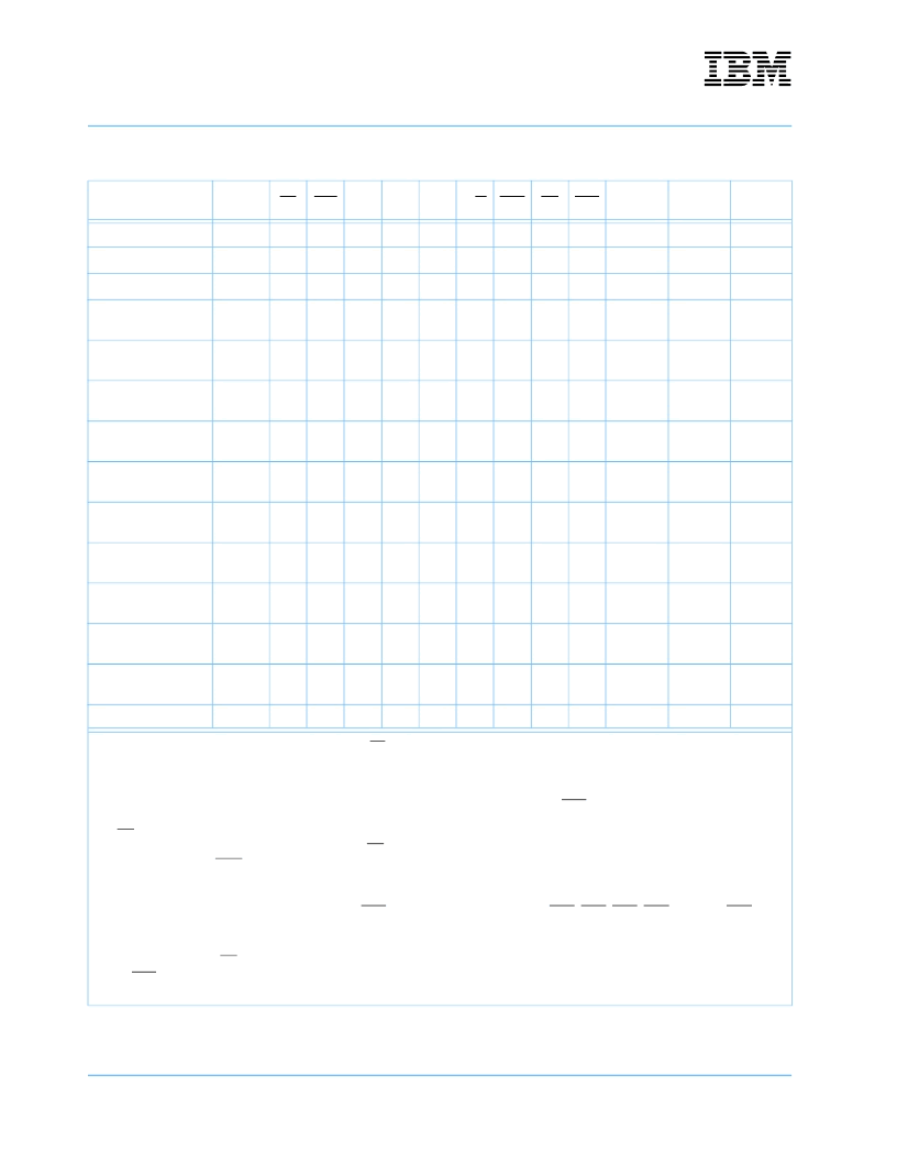
Cycle Definition Truth Table
Operation
Address
used
CE
CE2
CE2
ZZ
ADV/
LD
R/W
BWx
OE
CKE
CLK
DQ
Notes
Deselect Cycle
None
H
X
X
L
L
X
X
X
L
L
→
H
High-Z
Deselect Cycle
None
X
H
X
L
L
X
X
X
L
L
→
H
High-Z
Deselect Cycle
None
X
X
L
L
L
X
X
X
L
L
→
H
High-Z
Deselect Cycle
(Continue)
None
X
X
X
L
H
X
X
X
L
L
→
H
High-Z
1
Read Cycle
(Begin Burst)
External
L
L
H
L
L
H
X
L
L
L
→
H
Q
Read Cycle
(Continue Burst)
Next
X
X
X
L
H
X
X
L
L
L
→
H
Q
1, 2
No Op /Dummy Read
(Begin Burst)
External
L
L
H
L
L
H
X
H
L
L
→
H
High-Z
3
Dummy Read
(Continue Burst)
Next
X
X
X
L
H
X
X
H
L
L
→
H
High-Z
1, 2, 3
Write Cycle
(Begin Burst)
External
L
L
H
L
L
L
L
X
L
L
→
H
D
4
Write Cycle
(Continue Burst)
Next
X
X
X
L
H
X
L
X
L
L
→
H
D
1, 2, 4
No Op /Write Abort
(Begin Burst)
None
L
L
H
L
L
L
H
X
L
L
→
H
High-Z
3, 4
Write Abort
(Continue Burst)
Next
X
X
X
L
H
X
H
X
L
L
→
H
High-Z
1, 2, 3, 4
Clock Disabled
(Stall)
Current
X
X
X
L
X
X
X
X
H
L
→
H
Held
5
Sleep Mode
None
X
X
X
H
X
X
X
X
X
X
High-Z
1. Continue Burst Cycles are initiated with the ADV/LD pin held high. The type of cycle that is performed (Deselect, Read or Write) is
determined by the initial Deselect or Begin Read/Write burst cycle.
2. The address counter is incremented for all Continue Burst cycles (see Interleaved Burst Sequence Truth Table on page 7 and Lin-
ear Burst Sequence Truth Table on page 7 for Burst order and wrap information).
3. Dummy Read and Write Abort cycles can be considered Non-Operations or
“
NOP.
”
All BWx inputs must be High to prevent a Write
operation from being performed.
4. OE may be tied low to reduce the number of control pins for the SRAM. The device will automatically tri-state the output drivers
during a Write cycle. By carefully controlling the OE timings, cycle time improvements can be obtained.
5. If a Clock Disable (CKE = High) command is issued during a Read operation, the DQ bus will remain active (Low-Z). If it occurs
during a Write operation, the bus will remain inactive (High-Z), and any pending Data-In is delayed by an additional cycle. No oper-
ation will be performed during the Clock Disable cycle.
X=Don
’
t Care, H=Logic High, L= Logic Low. BWx=H means all byte write inputs (BWa, BWb, BWc, BWd) are High. BWx=L
means one or more byte write signals are Low. (See Read/Write Command Truth Table on page 7 for more information on
byte enable control).
All inputs except OE and ZZ must meet setup and hold times around the rising edge of CLK
CKE held High will insert wait states. Internal device registers will hold their previous values.
On-chip circuitry is included to ensure that outputs are held in High-Z during power-up.
相關(guān)PDF資料 |
PDF描述 |
|---|---|
| IBM0436A86LQKA | 8 Mb Synchronous Communication SRAM(8M位同步流水線式通訊靜態(tài)RAM) |
| IBM0436A86SQKA | 8 Mb Synchronous Communication SRAM(8M位同步流水線式通信靜態(tài)RAM) |
| IBM043614PQKB | 32K X 36 BURST SRAM(1M (32K X 36)同步可猝發(fā)高性能靜態(tài)RAM) |
| IBM11E4480BG | 4M x 36 ECC-on-SIMM(single in-line memory module)(4M x 36 片上帶可兼容的糾錯代碼的單列動態(tài)RAM模塊) |
| IBM11D4480BG | 4M x 36 ECC-on-SIMM(single in-line memory module)(4M x 36 片上帶可兼容的糾錯代碼的單列動態(tài)RAM模塊) |
相關(guān)代理商/技術(shù)參數(shù) |
參數(shù)描述 |
|---|---|
| IBM043610QLAB4H | 制造商:IBM 功能描述:* |
| IBM043611TLAB4 | 制造商:IBM 功能描述: |
| IBM043612PQK-11 | 制造商:IBM 功能描述:Synchronous SRAM, 32K x 36, 100 Pin, Plastic, QFP |
| IBM043612PQKB10 | 制造商:IBM 功能描述:* |
| IBM043612PQKB8 | 制造商:IBM 功能描述:* |
發(fā)布緊急采購,3分鐘左右您將得到回復(fù)。