- 您現(xiàn)在的位置:買賣IC網(wǎng) > PDF目錄173638 > GS8640FZ18T-8IVT (GSI TECHNOLOGY) 4M X 18 ZBT SRAM, 8 ns, PQFP100 PDF資料下載
參數(shù)資料
| 型號: | GS8640FZ18T-8IVT |
| 廠商: | GSI TECHNOLOGY |
| 元件分類: | SRAM |
| 英文描述: | 4M X 18 ZBT SRAM, 8 ns, PQFP100 |
| 封裝: | TQFP-100 |
| 文件頁數(shù): | 19/19頁 |
| 文件大小: | 456K |
| 代理商: | GS8640FZ18T-8IVT |
GS8640FZ18/36T-xxxV
Specifications cited are subject to change without notice. For latest documentation see http://www.gsitechnology.com.
Rev: 1.00a 2/2009
9/19
2007, GSI Technology
Burst Cycles
Although NBT RAMs are designed to sustain 100% bus bandwidth by eliminating turnaround cycle when there is transition from
read to write, multiple back-to-back reads or writes may also be performed. NBT SRAMs provide an on-chip burst address
generator that can be utilized, if desired, to further simplify burst read or write implementations. The ADV control pin, when
driven high, commands the SRAM to advance the internal address counter and use the counter generated address to read or write
the SRAM. The starting address for the first cycle in a burst cycle series is loaded into the SRAM by driving the ADV pin low, into
Load mode.
Burst Order
The burst address counter wraps around to its initial state after four addresses (the loaded address and three more) have been
accessed. The burst sequence is determined by the state of the Linear Burst Order pin (LBO). When this pin is low, a linear burst
sequence is selected. When the RAM is installed with the LBO pin tied high, Interleaved burst sequence is selected. See the tables
below for details.
Note:
There is a pull-down device on the ZZ pin, so this input pin can be unconnected and the chip will operate in the default states as specified in
the above tables.
Burst Counter Sequences
BPR 1999.05.18
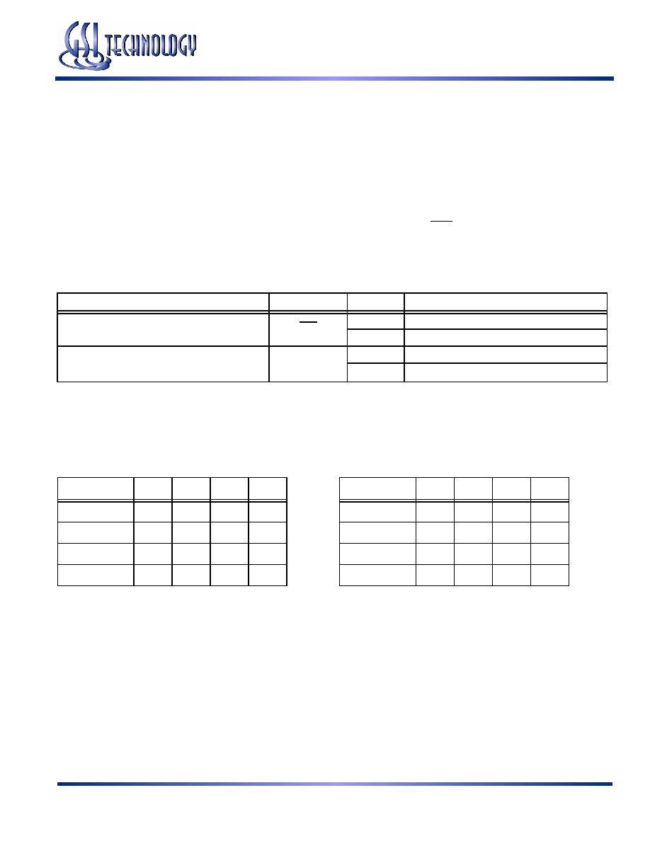
Mode Pin Functions
Mode Name
Pin Name
State
Function
Burst Order Control
LBO
L
Linear Burst
H
Interleaved Burst
Power Down Control
ZZ
L or NC
Active
H
Standby, IDD = ISB
Note:
The burst counter wraps to initial state on the 5th clock.
Note:
The burst counter wraps to initial state on the 5th clock.
Linear Burst Sequence
A[1:0] A[1:0] A[1:0] A[1:0]
1st address
00
01
10
11
2nd address
01
10
11
00
3rd address
10
11
00
01
4th address
11
00
01
10
Interleaved Burst Sequence
A[1:0] A[1:0] A[1:0] A[1:0]
1st address
00
01
10
11
2nd address
01
00
11
10
3rd address
10
11
00
01
4th address
11
10
01
00
相關(guān)PDF資料 |
PDF描述 |
|---|---|
| GS8642Z36GF-167T | 2M X 36 ZBT SRAM, 8 ns, PBGA165 |
| GS8642ZV36E-167IT | 2M X 36 ZBT SRAM, 8 ns, PBGA165 |
| GS8662D11BGD-400 | 8M X 9 STANDARD SRAM, 0.45 ns, PBGA165 |
| GS8662D36BD-300IT | 2M X 36 STANDARD SRAM, 0.45 ns, PBGA165 |
| GS8662DT10BGD-400IT | 8M X 9 QDR SRAM, 0.45 ns, PBGA165 |
相關(guān)代理商/技術(shù)參數(shù) |
參數(shù)描述 |
|---|---|
| GS8640FZ36GT-5.5 | 制造商:GSI Technology 功能描述:SRAM SYNC QUAD 3.3V 72MBIT 2MX36 5.5NS 100TQFP - Trays |
| GS8640FZ36GT-6.5 | 制造商:GSI Technology 功能描述:SRAM SYNC QUAD 3.3V 72MBIT 2MX36 6.5NS 100TQFP - Trays |
| GS8640FZ36GT-7.5 | 制造商:GSI Technology 功能描述:SRAM SYNC QUAD 3.3V 72MBIT 2MX36 7.5NS 100TQFP - Trays |
| GS8640FZ36GT-8.0 | 制造商:GSI Technology 功能描述:SRAM SYNC QUAD 3.3V 72MBIT 2MX36 8NS 100TQFP - Trays |
| GS8640FZ36GT-8.0I | 制造商:GSI Technology 功能描述:SRAM SYNC QUAD 3.3V 72MBIT 2MX36 8NS 100TQFP - Trays |
發(fā)布緊急采購,3分鐘左右您將得到回復(fù)。