- 您現(xiàn)在的位置:買(mǎi)賣IC網(wǎng) > PDF目錄223865 > GS81302TT07E-333IT (GSI TECHNOLOGY) 16M X 8 DDR SRAM, 0.45 ns, PBGA165 PDF資料下載
參數(shù)資料
| 型號(hào): | GS81302TT07E-333IT |
| 廠商: | GSI TECHNOLOGY |
| 元件分類: | SRAM |
| 英文描述: | 16M X 8 DDR SRAM, 0.45 ns, PBGA165 |
| 封裝: | 15 X 17 MM, 1 MM PITCH, FPBGA-165 |
| 文件頁(yè)數(shù): | 19/31頁(yè) |
| 文件大?。?/td> | 1198K |
| 代理商: | GS81302TT07E-333IT |
第1頁(yè)第2頁(yè)第3頁(yè)第4頁(yè)第5頁(yè)第6頁(yè)第7頁(yè)第8頁(yè)第9頁(yè)第10頁(yè)第11頁(yè)第12頁(yè)第13頁(yè)第14頁(yè)第15頁(yè)第16頁(yè)第17頁(yè)第18頁(yè)當(dāng)前第19頁(yè)第20頁(yè)第21頁(yè)第22頁(yè)第23頁(yè)第24頁(yè)第25頁(yè)第26頁(yè)第27頁(yè)第28頁(yè)第29頁(yè)第30頁(yè)第31頁(yè)
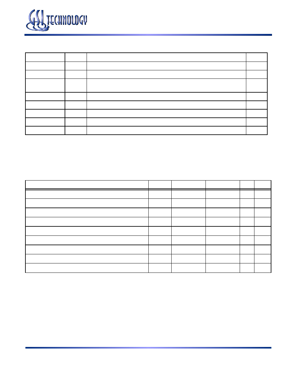
JTAG TAP Instruction Set Summary
Instruction
Code
Description
Notes
EXTEST
000
Places the Boundary Scan Register between TDI and TDO.
1
IDCODE
001
Preloads ID Register and places it between TDI and TDO.
1, 2
SAMPLE-Z
010
Captures I/O ring contents. Places the Boundary Scan Register between TDI and TDO.
Forces all RAM output drivers to High-Z.
1
GSI
011
GSI private instruction.
1
SAMPLE/PRELOAD
100
Captures I/O ring contents. Places the Boundary Scan Register between TDI and TDO.
1
GSI
101
GSI private instruction.
1
GSI
110
GSI private instruction.
1
BYPASS
111
Places Bypass Register between TDI and TDO.
1
Notes:
1. Instruction codes expressed in binary, MSB on left, LSB on right.
2. Default instruction automatically loaded at power-up and in test-logic-reset state.
GS81302TT07/10/19/37E-450/400/350/333/300
Specifications cited are subject to change without notice. For latest documentation see http://www.gsitechnology.com.
Rev: 1.00 5/2011
26/31
2011, GSI Technology
JTAG Port Recommended Operating Conditions and DC Characteristics
Parameter
Symbol
Min.
Max.
Unit
Notes
Test Port Input Low Voltage
VILJ
–0.3
0.3 * VDD
V
1
Test Port Input High Voltage
VIHJ
0.7 * VDD
VDD +0.3
V
1
TMS, TCK and TDI Input Leakage Current
IINHJ
–300
1
uA
2
TMS, TCK and TDI Input Leakage Current
IINLJ
–1
100
uA
3
TDO Output Leakage Current
IOLJ
–1
1
uA
4
Test Port Output High Voltage
VOHJ
VDD – 0.2
—
V
5, 6
Test Port Output Low Voltage
VOLJ
—
0.2
V
5, 7
Test Port Output CMOS High
VOHJC
VDD – 0.1
—
V
5, 8
Test Port Output CMOS Low
VOLJC
—
0.1
V
5, 9
Notes:
1. Input Under/overshoot voltage must be –1 V < Vi < VDDn +1 V not to exceed 2.9 V maximum, with a pulse width not to exceed 20% tTKC.
2. VILJ ≤ VIN ≤ VDDn
3. 0 V
≤ VIN ≤ VILJn
4. Output Disable, VOUT = 0 to VDDn
5. The TDO output driver is served by the VDD supply.
6. IOHJ = –2 mA
7. IOLJ = + 2 mA
8. IOHJC = –100 uA
9. IOLJC = +100 uA
相關(guān)PDF資料 |
PDF描述 |
|---|---|
| GS81302TT07GE-333I | 16M X 8 DDR SRAM, 0.45 ns, PBGA165 |
| GS816036AGT-250I | 512K X 36 CACHE SRAM, 5.5 ns, PQFP100 |
| GS8160E36GT-250 | 512K X 36 CACHE SRAM, 5.5 ns, PQFP100 |
| GS816118AGT-200IT | 1M X 18 CACHE SRAM, 6.5 ns, PQFP100 |
| GS8161E18GT-166I | 1M X 18 CACHE SRAM, 7 ns, PQFP100 |
相關(guān)代理商/技術(shù)參數(shù) |
參數(shù)描述 |
|---|---|
| GS815018AB | 制造商:GSI 制造商全稱:GSI Technology 功能描述:1M x 18, 512K x 36 18Mb Register-Register Late Write SRAM |
| GS815018AB-250 | 制造商:GSI Technology 功能描述:SRAM SYNC DUAL 2.5V 18MBIT 1MX18 2NS 119FPBGA - Trays |
| GS815018AB-250I | 制造商:GSI Technology 功能描述:SRAM SYNC DUAL 2.5V 18MBIT 1MX18 2NS 119FPBGA - Trays |
| GS815018AB-300 | 制造商:GSI Technology 功能描述:SRAM SYNC DUAL 2.5V 18MBIT 1MX18 1.6NS 119FPBGA - Trays |
| GS815018AB-300I | 制造商:GSI Technology 功能描述:SRAM SYNC DUAL 2.5V 18MBIT 1MX18 1.6NS 119FPBGA - Trays |
發(fā)布緊急采購(gòu),3分鐘左右您將得到回復(fù)。