- 您現(xiàn)在的位置:買賣IC網(wǎng) > PDF目錄67505 > FMS9874AKGC140 (FAIRCHILD SEMICONDUCTOR CORP) 3-CH 8-BIT PROPRIETARY METHOD ADC, PARALLEL ACCESS, PQFP100 PDF資料下載
參數(shù)資料
| 型號(hào): | FMS9874AKGC140 |
| 廠商: | FAIRCHILD SEMICONDUCTOR CORP |
| 元件分類: | ADC |
| 英文描述: | 3-CH 8-BIT PROPRIETARY METHOD ADC, PARALLEL ACCESS, PQFP100 |
| 封裝: | MQFP-100 |
| 文件頁(yè)數(shù): | 22/26頁(yè) |
| 文件大小: | 454K |
| 代理商: | FMS9874AKGC140 |
第1頁(yè)第2頁(yè)第3頁(yè)第4頁(yè)第5頁(yè)第6頁(yè)第7頁(yè)第8頁(yè)第9頁(yè)第10頁(yè)第11頁(yè)第12頁(yè)第13頁(yè)第14頁(yè)第15頁(yè)第16頁(yè)第17頁(yè)第18頁(yè)第19頁(yè)第20頁(yè)第21頁(yè)當(dāng)前第22頁(yè)第23頁(yè)第24頁(yè)第25頁(yè)第26頁(yè)
PRODUCT SPECIFICATION
FMS9874A
5
REV. 1.2.10 1/14/02
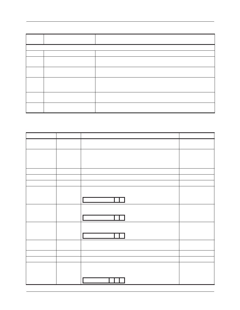
Pin Descriptions
Addressable Memory
Register Map
Pin
Name
Pin No.
Pin Function Description
Power and Ground
VDDA
3, 5, 9, 11, 14, 16, 95, 99, 100 ADC Supply Voltages. Provide a quiet noise free voltage.
VDDP
24, 25, 31, 36, 38
PLL Supply Voltage. Most sensitive supply voltage. Provide a very
quiet noise free voltage.
VDDO
50, 60, 62, 72, 85, 91
Digital Output Supply Voltage. Decouple judiciously to avoid
propagation of switching noise.
GND
1, 4, 6, 10, 12, 15, 17, 26, 27,
30, 35, 37, 39, 40, 41, 49, 59,
61, 71, 84, 90, 92, 93, 94
Ground. Returns for all power supplies. Connect ground pins to a
solid ground-plane.
VREFIN
98
Voltage Reference Input. Common reference input to RGB
converters. Connect to VREFOUT, if internal reference is used.
VREFOUT
97
Voltage Reference Output. Internal band-gap reference output. Tie to
ground through a 0.1F capacitor.
Name
Address
Function
Default (hex)
PLLN11-4
00
PLL divide ratio, MSBs. PLLN + 1 = total number of
pixels per horizontal line.
69 (1693)
PLLCTRL
01
PLL Control Register.
1. Lower four bits of PLL divide ratio.
2. PLL Subdivide phase.
3. PLL Subdivide ratio.
D0 (1693)
GR7-0
02
Gain, red channel. Adjustable from 70 to 140%.
80
GG7-0
03
Gain, green channel. Adjustable from 70 to 140%.
80
GB7-0
04
Gain, blue channel. Adjustable from 70 to 140%.
80
OSR5-0
05
Offset, red channel. OSR5-0 is stored in the six upper
register bits 7-2.Default value is decimal 32.
80
OSG5-0
06
Offset, green channel. OSR5-0 is stored in the six upper
register bits 7-2. Default value is decimal 32.
80
OSB5-0
07
Offset, blue channel. OSR5-0 is stored in the six upper
register bits 7-2. Default value is decimal 32.
80
CD7-0
08
Clamp delay. Delay in pixels from trailing edge of
horizontal sync.
80
CW7-0
09
Clamp width. Width of clamp pulse in pixels.
80
CONFIG 1
0A
Configuration Register No. 1
F4
PHASE7-0
0B
Sampling clock phase. PHASE4-0 stored in upper
register bits 7-3. PHASE sets the sampling clock phase in
11.25° increments. Default value is decimal 16.
80
OSR5–0
X X
OSG5–0
X X
OSB5–0
X X
PHASE4–0
X X X
相關(guān)PDF資料 |
PDF描述 |
|---|---|
| FMS9875KGC100 | 3-CH 8-BIT PROPRIETARY METHOD ADC, PARALLEL ACCESS, PQFP100 |
| FMS9875KGC100X | 3-CH 8-BIT PROPRIETARY METHOD ADC, PARALLEL ACCESS, PQFP100 |
| FMS9875KGC140 | 3-CH 8-BIT PROPRIETARY METHOD ADC, PARALLEL ACCESS, PQFP100 |
| FMS9875KGC140X | 3-CH 8-BIT PROPRIETARY METHOD ADC, PARALLEL ACCESS, PQFP100 |
| FN3410-10-44 | 500 V, 50 HZ, THREE PHASE EMI FILTER |
相關(guān)代理商/技術(shù)參數(shù) |
參數(shù)描述 |
|---|---|
| FMS9874KGC | 功能描述:視頻 IC RoHS:否 制造商:Fairchild Semiconductor 工作電源電壓:5 V 電源電流:80 mA 最大工作溫度:+ 85 C 封裝 / 箱體:TSSOP-28 封裝:Reel |
| FMS9874KGC100 | 制造商:FAIRCHILD 制造商全稱:Fairchild Semiconductor 功能描述:Graphics Digitizer - 3x8-Bit, 108Ms/s Triple Video A/D Converter with Clamps |
| FMS9875 | 制造商:FAIRCHILD 制造商全稱:Fairchild Semiconductor 功能描述:Triple 8-Bit, 108/140 MHz A/D Converter with Clamps and PLL |
| FMS9875KAC100 | 制造商:FAIRCHILD 制造商全稱:Fairchild Semiconductor 功能描述:Triple 8-Bit, 108/140 MHz A/D Converter with Clamps and PLL |
| FMS9875KAC140 | 制造商:FAIRCHILD 制造商全稱:Fairchild Semiconductor 功能描述:Triple 8-Bit, 108/140 MHz A/D Converter with Clamps and PLL |
發(fā)布緊急采購(gòu),3分鐘左右您將得到回復(fù)。