- 您現(xiàn)在的位置:買賣IC網(wǎng) > PDF目錄382961 > FM30C256 (Electronic Theatre Controls, Inc.) 12 AMP MINIATURE POWER RELAY PDF資料下載
參數(shù)資料
| 型號: | FM30C256 |
| 廠商: | Electronic Theatre Controls, Inc. |
| 英文描述: | 12 AMP MINIATURE POWER RELAY |
| 中文描述: | 256Kb的數(shù)據(jù)采集器 |
| 文件頁數(shù): | 3/18頁 |
| 文件大小: | 260K |
| 代理商: | FM30C256 |
Overview
The FM30C256 data collector combines a 256Kb
serial nonvolatile RAM with a real-time clock (RTC),
a power monitor, and a tamper detect circuit. The
FM30C256 integrates these complementary but
distinct functions under a common interface in a
single package. Despite providing multiple interface
Ids as explained below, the product is a single
monolithic device.
The memory is organized as 32Kx8 of FRAM and is
accessed via a separate 2-wire device ID from the
remaining functions. This allows the user to preserve
addressing information when switching between
memory and RTC functions. Modularity in software
design is preserved as well.
The real-time clock function and the tamper detection
is accessed under its own 2-wire device ID. This
allows clock data to be read while maintaining the
last (most recently used) memory address in the other
device. The clock and tamper functions are controlled
by 9 registers that are backed up by the external
battery. Clock and tamper functions continue to
operate from battery power when V
DD
drops below
the battery voltage.
In addition to the software-controlled functions, the
FM30C256 also provides reset signal for an external
microcontroller host. This signal is asserted when
V
DD
drops below the specified trip point (V
TP
). It
FM30C256
Rev 2.1
Dec. 2002
Page 3 of 18
remains asserted until V
DD
returns above V
TP
for the
hold-off period (t
RPU
). The power monitor has no
interaction with other software-controlled functions.
Any access to the device will be ignored when V
DD
<
V
TP
.
Memory Operation
When accessing the FM30C256, the user addresses
32,768 locations each with 8 data bits. These data bits
are shifted in and out serially. The 32,768 addresses
are accessed using the two-wire protocol, which
includes a slave address (to distinguish from other
non-memory devices), and an extended 16-bit
address. The decoder uses only the lower 15 bits for
accessing the memory. The upper address bit should
be set to 0 for compatibility with larger devices in the
future.
The memory is read or written at the speed of the
two-wire bus. The interface protocol is described
further below.
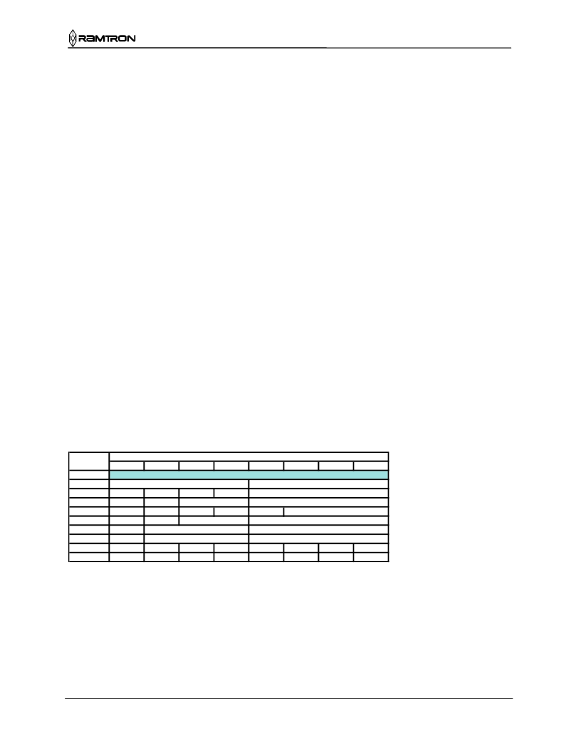
RTC Register Map
The interface to clock and tamper functions is via 9
address locations mapped to a separate 2-wire device
ID. The interface protocol is described below. The
registers contain timekeeping data, control bits, or
information flags. A short description of each register
follows. Detailed descriptions follow the register
summary section.
Register Map Summary Table
Data
Address
9-F
8
7
6
5
4
3
2
1
0
D7
D6
D5
D4
D3
D2
D1
D0
Function
Range
10 years
years
months
date
Years
Month
Date
Day
Hours
Minutes
Seconds
CAL/Control
Flags/Control
00-99
1-12
1-31
1-7
0-23
0-59
0-59
0
0
0
0
0
0
0
0
0
0
0
10 mo
10 date
0
0
0
day
10 hours
hours
minutes
seconds
CAL2
CAL
10 minutes
10 seconds
CALS
reserved
/OSCEN
Tamper
TSEN
CF
CAL4
reserved
CAL3
TST
CAL1
W
CAL0
R
ILLEGAL ADDRESSES
相關(guān)PDF資料 |
PDF描述 |
|---|---|
| FM30C256-S | 256Kb Data Collector |
| FM361 | 2mm TERMINAL STRIP |
| FM362 | 2mm TERMINAL STRIP |
| FM3808 | 4Kb FRAM Serial 3V Memory |
| FM3808-70-T | 4Kb FRAM Serial 3V Memory |
相關(guān)代理商/技術(shù)參數(shù) |
參數(shù)描述 |
|---|---|
| FM30C256-S | 功能描述:F-RAM 256K w/RTC Pwr Mon & Batt Switchover RoHS:否 存儲容量:512 Kbit 組織:64 K x 8 接口:SPI 工作電源電壓:2 V to 3.6 V 工作溫度范圍:- 40 C to + 85 C 安裝風(fēng)格:SMD/SMT 封裝 / 箱體:SOIC-8 封裝:Tube 制造商:Cypress Semiconductor |
| FM30C256-STR | 功能描述:F-RAM 256K w/RTC Pwr Mon & Batt Switchover RoHS:否 存儲容量:512 Kbit 組織:64 K x 8 接口:SPI 工作電源電壓:2 V to 3.6 V 工作溫度范圍:- 40 C to + 85 C 安裝風(fēng)格:SMD/SMT 封裝 / 箱體:SOIC-8 封裝:Tube 制造商:Cypress Semiconductor |
| FM30C350Q (550606) | 制造商:AMETEK Technical and Industrial Products 功能描述:Air Flow Meter, Analog, 3-in - 8.0 NPSC, 70-350 SCFM Flow Range, 2% Accuracy |
| FM30C475Q (550607) | 制造商:AMETEK Technical and Industrial Products 功能描述:Air Flow Meter, Analog, 3-in - 8.0 NPSC, 95-475 SCFM Flow Range, 2% Accuracy |
| FM30L250Q (550866) | 制造商:AMETEK Technical and Industrial Products 功能描述:Flow Meter, LCD Display in SCFM, 120VAC 50/60Hz Input, for 50-250 SCFM Flow Rate |
發(fā)布緊急采購,3分鐘左右您將得到回復(fù)。