- 您現(xiàn)在的位置:買賣IC網(wǎng) > PDF目錄67412 > FAN5019MTCX_NL (FAIRCHILD SEMICONDUCTOR CORP) SWITCHING CONTROLLER, 4000 kHz SWITCHING FREQ-MAX, PDSO28 PDF資料下載
參數(shù)資料
| 型號(hào): | FAN5019MTCX_NL |
| 廠商: | FAIRCHILD SEMICONDUCTOR CORP |
| 元件分類: | 穩(wěn)壓器 |
| 英文描述: | SWITCHING CONTROLLER, 4000 kHz SWITCHING FREQ-MAX, PDSO28 |
| 封裝: | LEAD FREE, TSSOP-28 |
| 文件頁數(shù): | 13/30頁 |
| 文件大?。?/td> | 781K |
| 代理商: | FAN5019MTCX_NL |
第1頁第2頁第3頁第4頁第5頁第6頁第7頁第8頁第9頁第10頁第11頁第12頁當(dāng)前第13頁第14頁第15頁第16頁第17頁第18頁第19頁第20頁第21頁第22頁第23頁第24頁第25頁第26頁第27頁第28頁第29頁第30頁
FAN5019
PRODUCT SPECIFICATION
20
REV. 1.0.7 1/5/04
Selecting a Standard Inductor
The companies listed below can provide design consultation
and deliver power inductors optimized for high power
applications upon request.
Power Inductor Manufacturers
Coilcraft
(847)639-6400
www.coilcraft.com
Coiltronics
(561)752-5000
www.coiltronics.com
Sumida Electric Company
(510) 668-0660
www.sumida.com
Vishay Intertechnology
(402) 563-6866
www.vishay.com
Output Droop Resistance
The design requires that the regulator output voltage
measured at the CPU pins drops when the output current
increases. The specied voltage drop corresponds to a DC
output resistance (RO).
The output current is measured by summing together the
voltage across each inductor and then passing the signal
through a low-pass lter. This summer-lter is the CS
amplier congured with resistors RPH(X) (summers), and
RCS and CCS (lter). The output resistance of the regulator is
set by the following equations, where RL is the DCR of the
output inductors:
One has the exibility of choosing either RCS or RPH(X).
It is best to select RCS equal to 100k
, and then solve for
RPH(X) by rearranging Equation 6.
Next, use Equation 7 to solve for CCS:
It is best to have a dual location for CCS in the layout so stan-
dard values can be used in parallel to get as close to the value
desired. For this example, choosing CCS to be 4.7nF is a
good choice. For best accuracy, CCS should be a 5% or 10%
NPO capacitor. A close standard 1% value for RPH(X) is
100k
.
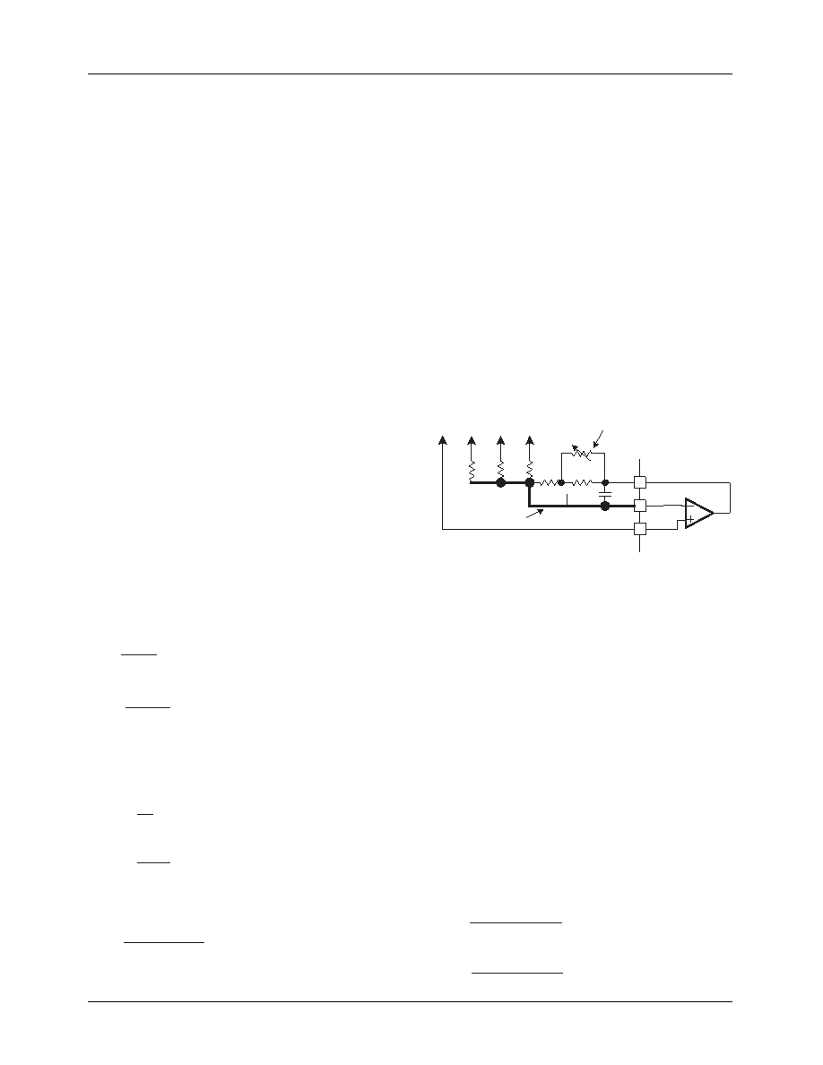
Inductor DCR Temperature Correction
With the inductor’s DCR being used as the sense element,
and copper wire being the source of the DCR, one needs to
compensate for temperature changes of the inductor’s wind-
ing. Fortunately, copper has a well-known temperature coef-
cient (TC) of 0.39%/°C.
If RCS is designed to have an opposite and equal percentage
change in resistance to that of the wire, it will cancel the
temperature variation of the inductor’s DCR. Due to the non-
linear nature of NTC thermistors, resistors RCS1 and RCS2
are needed (see Figure 5) to linearize the NTC and produce
the desired temperature tracking.
Figure 5. Temperature Compensation Circuit
The following procedure and expressions will yield values to
use for RCS1, RCS2, and RTH (the thermistor value at 25°C)
for a given RCS value.
1.
Select an NTC to be used based on type and value. Since
we do not have a value yet, start with a thermistor with a
value close to RCS. The NTC should also have an initial
tolerance of better than 5%.
2.
Based on the type of NTC, nd its relative resistance
value at two temperatures. The temperatures to use that
work well are 50°C and 90°C. We will call these resis-
tance values A (A is RTH(50°C)/RTH(25°C)) and B (B is
RTH(90°C)/RTH(25°C)). Note that the NTC’s relative value
is always 1 at 25°C.
3.
Next, nd the relative value of RCS required for each of
these temperatures. This is based on the percentage
change needed, which we will initially make 0.39%/°C.
We will call these r1 and r2 where:
L
X
PH
CS
O
R
×
=
)
(
(6)
CS
L
CS
R
L
C
×
=
(7)
CS
O
L
X
PH
R
×
=
)
(
=
×
=
k
m
R
X
PH
123
100
3
.
1
6
.
1
)
(
nF
k
m
nH
C
CS
06
.
4
100
6
.
1
650
=
×
=
18
17
16
CSREF
CSSUM
CSCOMP
CSA
C
CS
1.8nF
R
CS1
R
CS2
R
TH
R
PH1
R
PH3
R
PH2
Keep this path as
short as possible
and well away from
Switch Node lines
Place as close as
possible to nearest
inductor or low-side
MOSFET
To Switch Nodes
To V
OUT
sense
()
(
)
25
1
×
+
=
T
TC
r
()
(
)
25
1
2
×
+
=
T
TC
r
TC = 0.0039
T1 = 50°C
T2 = 90°C
相關(guān)PDF資料 |
PDF描述 |
|---|---|
| FAN5037MX_NL | SWITCHING CONTROLLER, PDSO8 |
| FAN5037M_NL | SWITCHING CONTROLLER, PDSO8 |
| FAN5061M | SWITCHING CONTROLLER, 345 kHz SWITCHING FREQ-MAX, PDSO20 |
| FAN5201MSA | 6 A BATTERY CHARGE CONTROLLER, 275 kHz SWITCHING FREQ-MAX, PDSO24 |
| FAN5361UMP10X | SWITCHING REGULATOR, DSO6 |
相關(guān)代理商/技術(shù)參數(shù) |
參數(shù)描述 |
|---|---|
| FAN501MPX | 制造商:Fairchild Semiconductor Corporation 功能描述:PWM CONTROLLER - Tape and Reel |
| FAN5020_AAC3116B WAF | 制造商:Fairchild Semiconductor Corporation 功能描述: |
| FAN5021_AAC3026B WAF | 制造商:Fairchild Semiconductor Corporation 功能描述: |
| FAN5026 | 制造商:FAIRCHILD 制造商全稱:Fairchild Semiconductor 功能描述:Dual DDR/Dual-output PWM Controller |
| FAN5026_11 | 制造商:FAIRCHILD 制造商全稱:Fairchild Semiconductor 功能描述:Dual DDR / Dual-Output PWM Controller |
發(fā)布緊急采購,3分鐘左右您將得到回復(fù)。