- 您現(xiàn)在的位置:買(mǎi)賣(mài)IC網(wǎng) > PDF目錄362753 > EPM9320A (Altera Corporation) Programmable Logic Device Family(MAX9000可編程邏輯系列器件) PDF資料下載
參數(shù)資料
| 型號(hào): | EPM9320A |
| 廠(chǎng)商: | Altera Corporation |
| 英文描述: | Programmable Logic Device Family(MAX9000可編程邏輯系列器件) |
| 中文描述: | 可編程邏輯器件系列(MAX9000可編程邏輯系列器件) |
| 文件頁(yè)數(shù): | 32/41頁(yè) |
| 文件大?。?/td> | 604K |
| 代理商: | EPM9320A |
第1頁(yè)第2頁(yè)第3頁(yè)第4頁(yè)第5頁(yè)第6頁(yè)第7頁(yè)第8頁(yè)第9頁(yè)第10頁(yè)第11頁(yè)第12頁(yè)第13頁(yè)第14頁(yè)第15頁(yè)第16頁(yè)第17頁(yè)第18頁(yè)第19頁(yè)第20頁(yè)第21頁(yè)第22頁(yè)第23頁(yè)第24頁(yè)第25頁(yè)第26頁(yè)第27頁(yè)第28頁(yè)第29頁(yè)第30頁(yè)第31頁(yè)當(dāng)前第32頁(yè)第33頁(yè)第34頁(yè)第35頁(yè)第36頁(yè)第37頁(yè)第38頁(yè)第39頁(yè)第40頁(yè)第41頁(yè)
32
Altera Corporation
MAX 9000 Programmable Logic Device Family Data Sheet
Notes to tables:
(1)
These values are specified under the MAX 9000 device recommended operating conditions, shown in
Table 12 on
page 24
.
(2)
See
Application Note 77 (Understanding MAX 9000 Timing)
in this data book for more information on test conditions
for
t
PD1
and
t
PD2
delays.
(3)
This parameter is a guideline that is sample-tested only. It is based on extensive device characterization. This
parameter applies for both global and array clocking as well as both macrocell and I/O cell registers.
(4)
Measured with a 16-bit loadable, enabled, up/down counter programmed in each LAB.
(5)
The
t
LPA
parameter must be added to the
t
LOCAL
parameter for macrocells running in low-power mode
.
(6)
The
t
ROW
,
t
COL,
and
t
IOC
delays are worst-case values for typical applications. Post-compilation timing simulation
or timing analysis is required to determine actual worst-case performance.
Power
Consumption
The supply power (P) versus frequency (
f
MAX
) for MAX 9000 devices can
be calculated with the following equation:
P = P
INT
+ P
IO
= I
CCINT
×
V
CC
+ P
IO
The P
IO
value, which depends on the device output load characteristics
and switching frequency, can be calculated using the guidelines given in
Application Note 74 (Evaluating Power for Altera Devices)
in this data book.
The I
CCINT
value depends on the switching frequency and the application
logic.
The I
CCINT
value is calculated with the following equation:
I
CCINT
= (A
×
MC
TON
) + [B
×
(MC
DEV
–
MC
TON
)] + (C
×
MC
USED
×
f
MAX
×
tog
LC
)
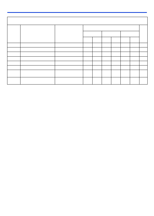
Table 21. Interconnect Delays
Symbol
Parameter
Conditions
Speed Grade
Unit
-10
-15
-20
Min
Max
Min
Max
Min
Max
t
LOCAL
t
ROW
t
COL
t
DIN_D
t
DIN_CLK
t
DIN_CLR
t
DIN_IOC
LAB local array delay
0.5
0.5
0.5
ns
ns
ns
ns
ns
ns
ns
FastTrack row delay
(6)
0.9
1.4
2.0
FastTrack column delay
(6)
0.9
1.7
3.0
Dedicated input data delay
4.0
4.5
5.0
Dedicated input clock delay
2.7
3.5
4.0
Dedicated input clear delay
4.5
5.0
5.5
Dedicated input I/O register
clock delay
2.5
3.5
4.5
t
DIN_IO
Dedicated input I/O register
control delay
5.5
6.0
6.5
ns
相關(guān)PDF資料 |
PDF描述 |
|---|---|
| EPM9480 | Programmable Logic Device Family(MAX9000可編程邏輯系列器件) |
| EPM9320 | Programmable Logic Device Family(MAX9000可編程邏輯系列器件) |
| EPM9400 | Programmable Logic Device Family(MAX9000可編程邏輯系列器件) |
| EPM9560 | Programmable Logic Device Family(MAX9000可編程邏輯系列器件) |
| EPM9560A | Programmable Logic Device Family(MAX9000可編程邏輯系列器件) |
相關(guān)代理商/技術(shù)參數(shù) |
參數(shù)描述 |
|---|---|
| EPM9320ABC356-10 | 制造商:Rochester Electronics LLC 功能描述:- Bulk |
| EPM9320ABI356-10 | 制造商:未知廠(chǎng)家 制造商全稱(chēng):未知廠(chǎng)家 功能描述: |
| EPM9320ALC84-10 | 制造商:Altera Corporation 功能描述:IC MAX |
| EPM9320ALC84-10N | 制造商:Altera Corporation 功能描述:IC MAX |
| EPM9320ALI84-10 | 制造商:Altera Corporation 功能描述:IC MAX 84PLCC 制造商:Altera Corporation 功能描述:IC CPLD 320MC 10NS 84PLCC |
發(fā)布緊急采購(gòu),3分鐘左右您將得到回復(fù)。