- 您現(xiàn)在的位置:買賣IC網(wǎng) > PDF目錄362657 > ELANSC410-66AI (ADVANCED MICRO DEVICES INC) Single-Chip, Low-Power, PC/AT-Compatible Microcontrollers PDF資料下載
參數(shù)資料
| 型號: | ELANSC410-66AI |
| 廠商: | ADVANCED MICRO DEVICES INC |
| 元件分類: | 微控制器/微處理器 |
| 英文描述: | Single-Chip, Low-Power, PC/AT-Compatible Microcontrollers |
| 中文描述: | 32-BIT, FLASH, 66 MHz, MICROCONTROLLER, PBGA292 |
| 封裝: | PLASTIC, BGA-292 |
| 文件頁數(shù): | 62/132頁 |
| 文件大小: | 2400K |
| 代理商: | ELANSC410-66AI |
第1頁第2頁第3頁第4頁第5頁第6頁第7頁第8頁第9頁第10頁第11頁第12頁第13頁第14頁第15頁第16頁第17頁第18頁第19頁第20頁第21頁第22頁第23頁第24頁第25頁第26頁第27頁第28頁第29頁第30頁第31頁第32頁第33頁第34頁第35頁第36頁第37頁第38頁第39頁第40頁第41頁第42頁第43頁第44頁第45頁第46頁第47頁第48頁第49頁第50頁第51頁第52頁第53頁第54頁第55頁第56頁第57頁第58頁第59頁第60頁第61頁當前第62頁第63頁第64頁第65頁第66頁第67頁第68頁第69頁第70頁第71頁第72頁第73頁第74頁第75頁第76頁第77頁第78頁第79頁第80頁第81頁第82頁第83頁第84頁第85頁第86頁第87頁第88頁第89頁第90頁第91頁第92頁第93頁第94頁第95頁第96頁第97頁第98頁第99頁第100頁第101頁第102頁第103頁第104頁第105頁第106頁第107頁第108頁第109頁第110頁第111頁第112頁第113頁第114頁第115頁第116頁第117頁第118頁第119頁第120頁第121頁第122頁第123頁第124頁第125頁第126頁第127頁第128頁第129頁第130頁第131頁第132頁
62
élanSC400 and élanSC410 Microcontrollers Data Sheet
SIGNAL DESCRIPTIONS
The descriptions in Table 19 are organized in
alphabetical order within the functional group listed here.
I
System Interface on page 62
I
Configuration Pins on page 63
I
Memory Interface on page 64
I
VL-Bus Interface on page 64
I
Power Management on page 65
I
Clocks on page 66
I
Parallel Port on page 66
I
Serial Port on page 66
I
Keyboard Interfaces on page 67
I
General-Purpose Input/Output on page 67
I
Serial Infrared Port on page 67
I
PC Card Controller (élanSC400 Microcontroller
Only) on page 67
I
LCD Graphics Controller (élanSC400 Microcontrol-
ler Only) on page 68
I
Boundary Scan Test Interface on page 69
I
Reset and Power on page 69
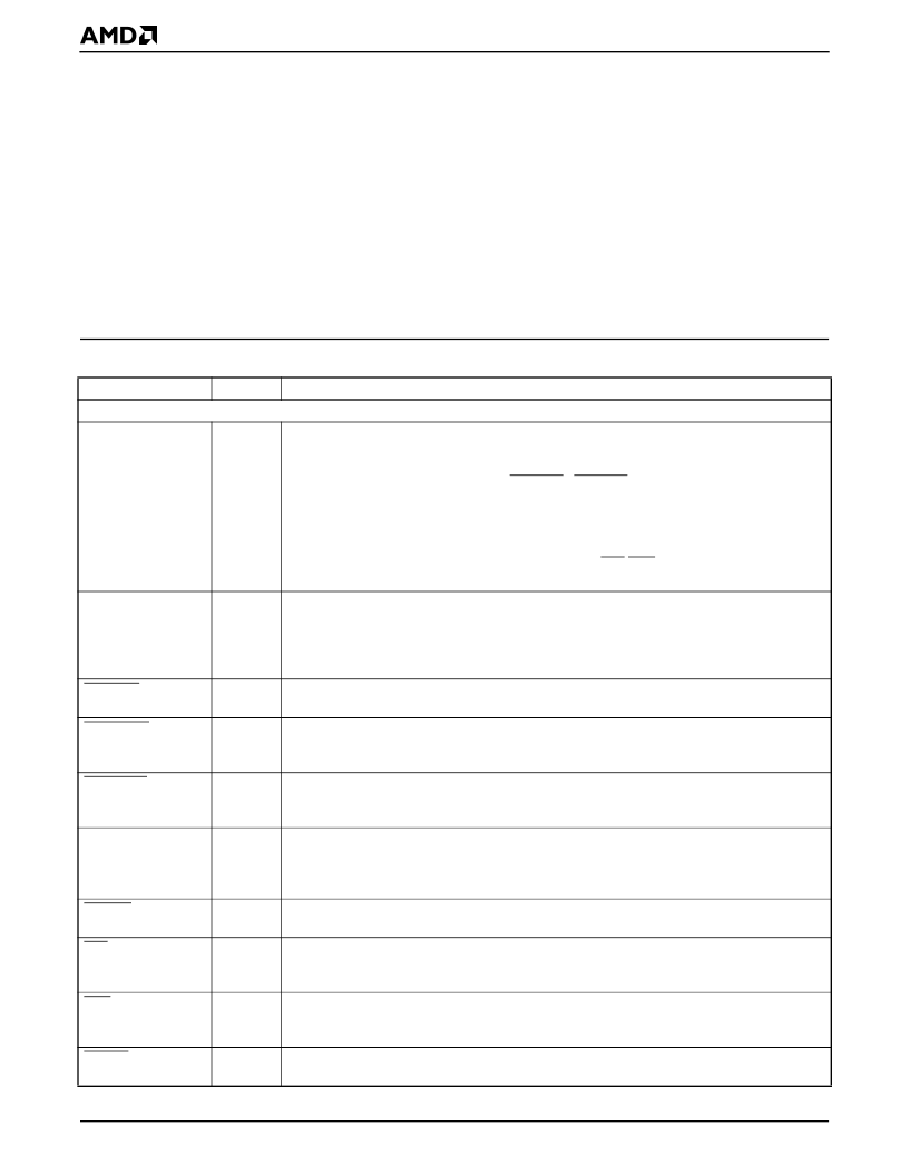
Table 19.
Signal Description Table
Signal
System Interface
AEN
Type
Description
O
DMA Address Enable
indicates that the current address active on the SA25–SA0 address
bus is a memory address, and that the current cycle is a DMA cycle. All I/O devices should
use this signal in decoding their I/O addresses, and should not respond when this signal is
asserted. When AEN is asserted, the PDACK1– PDACK0 signals are used to select the
appropriate I/O device for the DMA transfer. AEN is also asserted when a DMA cycle is
occurring internal to the chip.
On the élanSC400 microcontroller, AEN is also asserted for all accesses to the PC Card I/O
space to prevent ISA devices from responding to the IOR/IOW signal assertions because
these signals are shared between the PC Card and ISA interfaces.
Bus Address Latch Enable
is driven at the beginning of an ISA bus cycle with a valid
address. This signal can be used by external devices to latch the address for the current
cycle. BALE is also asserted for all accesses to the PC Card interfaces (memory or I/O)
(élanSC400 microcontroller only) and all DMA cycles. This prevents an ISA device from
responding to a cycle based on a previously latched address.
Data Buffer Output Enable
controls the output enable on the external transceiver required
to drive the peripheral data bus in local bus and 32-bit DRAM modes.
High Byte Data Buffer Direction Control
controls direction of data flow through the external
transceiver required to drive the peripheral data bus in local bus and 32-bit DRAM mode. This
is the control signal for the upper 8 bits of the data bus.
Low Byte Data Buffer Direction Control
controls direction of data flow through the external
transceiver required to drive the peripheral data bus in local bus and 32-bit DRAM mode. This
is the control signal for the lower 8 bits of the data bus.
I/O Channel Ready
should be driven by open-drain devices. When pulled Low during an ISA
access, wait states are inserted in the current cycle. This pin has an internal weak pullup that
should be supplemented by a stronger external pullup (usually 4.7 K
to 1 K
) for faster rise
time.
I/O Chip Select 16:
The targeted I/O device drives this signal active early in the cycle to
request a 16-bit transfer.
I/O Read Command
indicates that the current cycle is a read from the currently addressed
I/O device. When this signal is asserted, the selected I/O device can drive data onto the data
bus. This signal is also shared with the PC Card interface on the élanSC400 microcontroller.
I/O Write Command
indicates that the current cycle is a write to the currently addressed
I/O device. When this signal is asserted, the selected I/O device can latch data from the data
bus. This signal is also shared with the PC Card interface on the élanSC400 microcontroller.
Memory Chip Select
16
indicates to the ISA control logic that the targeted memory device
is a 16-bit-wide device.
BALE
O
DBUFOE
O
DBUFRDH
O
DBUFRDL
O
IOCHRDY
STI
PU
IOCS16
I
IOR
O
IOW
O
MCS16
I
相關PDF資料 |
PDF描述 |
|---|---|
| ELANSC400ANDELANSC410 | Single Synchronous Buck Pulse-Width Modulation (PWM) Controller; Temperature Range: 0°C to 70°C; Package: 14-SOIC T&R |
| ELANSC400 | Single-Chip, Low-Power, PC/AT-Compatible Microcontrollers |
| ELANSC400-100AC | Single-Chip, Low-Power, PC/AT-Compatible Microcontrollers |
| ELANSC520 | Microcontroller |
| ELC-10PR | HIGH-DENSITY SIGNAL CONDITIONERS 10-PACK PULSE SCALER |
相關代理商/技術參數(shù) |
參數(shù)描述 |
|---|---|
| ELANSC520 | 制造商:AMD 制造商全稱:Advanced Micro Devices 功能描述:Microcontroller |
| ELANSC520100AC | 制造商:Advanced Micro Devices 功能描述: |
| ELANSC520-100AC | 制造商:Advanced Micro Devices 功能描述:MCU 32-bit Elan RISC ROMLess 388-Pin BGA 制造商:Advanced Micro Devices 功能描述:PLASTIC BGA, CAVITY UP(BGA) - Trays 制造商:AMD (Advanced Micro Devices) 功能描述:MCU 32-bit Elan RISC ROMLess 388-Pin BGA |
| ELANSC520-100AD | 制造商:Advanced Micro Devices 功能描述:MCU 32-bit Elan RISC ROMLess 388-Pin BGA 制造商:AMD (Advanced Micro Devices) 功能描述:MCU 32-bit Elan RISC ROMLess 388-Pin BGA |
| ELANSC520-100AF | 制造商:Advanced Micro Devices 功能描述:Elansc520 microcontroller integrated 32-bit microcontroller with PC/AT-compatible peripherals, PCI host bridge 制造商:AMD (Advanced Micro Devices) 功能描述:Elansc520 microcontroller integrated 32-bit microcontroller with PC/AT-compatible peripherals, PCI host bridge |
發(fā)布緊急采購,3分鐘左右您將得到回復。