- 您現(xiàn)在的位置:買賣IC網(wǎng) > PDF目錄378593 > DSP56721 (飛思卡爾半導體(中國)有限公司) SymphonyTM DSP56720 / DSP56721 Multi-Core Audio Processors PDF資料下載
參數(shù)資料
| 型號: | DSP56721 |
| 廠商: | 飛思卡爾半導體(中國)有限公司 |
| 英文描述: | SymphonyTM DSP56720 / DSP56721 Multi-Core Audio Processors |
| 中文描述: | SymphonyTM DSP56720 / DSP56721多核音頻處理器 |
| 文件頁數(shù): | 15/54頁 |
| 文件大小: | 671K |
| 代理商: | DSP56721 |
第1頁第2頁第3頁第4頁第5頁第6頁第7頁第8頁第9頁第10頁第11頁第12頁第13頁第14頁當前第15頁第16頁第17頁第18頁第19頁第20頁第21頁第22頁第23頁第24頁第25頁第26頁第27頁第28頁第29頁第30頁第31頁第32頁第33頁第34頁第35頁第36頁第37頁第38頁第39頁第40頁第41頁第42頁第43頁第44頁第45頁第46頁第47頁第48頁第49頁第50頁第51頁第52頁第53頁第54頁
Symphony
TM
DSP56720 / DSP56721 Multi-Core Audio Processors, Rev.1
Freescale Semiconductor
15
19
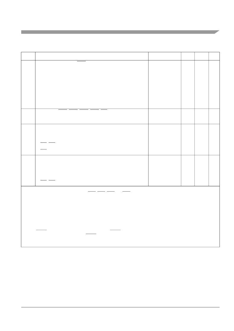
Duration of level sensitive IRQA assertion to ensure interrupt service
(when exiting Stop)
1, 2, 3
PLL is active during Stop and Stop delay is enabled (OMR Bit 6 = 0)
(
128K
×
T
C)
25
×
T
C
655
–
μ
s
PLL is active during Stop and Stop delay is not enabled (OMR Bit 6 =
1)
125
–
ns
PLL is not active during Stop and Stop delay is enabled (OMR Bit 6 =
0)
(128K x T
C
) +
T
LOCK
855
–
μ
s
PLL is not active during Stop and Stop delay is not enabled (OMR Bit
6 = 1)
(25 x T
C
) + T
LOCK
200
–
μ
s
20
Delay from IRQA, IRQB, IRQC, IRQD, NMI assertion to
general-purpose transfer output valid caused by first interrupt
instruction execution
1
10 x T
C
+ 3.8
–
53.8
ns
21
Interrupt Requests Rate
1
ESAI, ESAI_1, ESAI_2, ESAI_3, SHI, SHI_1, Timer, Timer_1
12 x T
C
–
60.0
ns
DMA
8 x T
C
–
40.0
ns
IRQ, NMI (edge trigger)
8 x T
C
–
40.0
ns
IRQ (level trigger)
12 x T
C
–
60.0
ns
22
DMA Requests Rate
Data read from ESAI, ESAI_1, ESAI_2, ESAI_3, SHI, SHI_1
6 x T
C
–
30.0
ns
Data write to ESAI, ESAI_1, ESAI_2, ESAI_3, SHI, SHI_1
7 x T
C
–
35.0
ns
Timer, Timer_1
2 x T
C
–
10.0
ns
IRQ, NMI (edge trigger)
3 x T
C
–
15.0
ns
Notes:
1.
When using fast interrupts and when IRQA, IRQB, IRQC, and IRQD are defined as level-sensitive, timings 19 through 21 apply to
prevent multiple interrupt service. To avoid these timing restrictions, the Edge-triggered mode is recommended when using fast
interrupts. Long interrupts are recommended when using Level-sensitive mode.
2.
For PLL disable, if using an external clock (PCTL Bit 13 = 1), no stabilization delay is required and recovery time will be defined by
the OMR Bit 6 settings.
For PLL enable, (if bit 12 of the PCTL register is 0), the PLL is shut down during Stop. Recovering from Stop requires the PLL to get
locked. The PLL lock procedure duration, PLL Lock Cycles (PLC), may be in the range of 200
μ
s.
3.
Periodically sampled and not 100% tested.
4.
RESET duration is measured during the time in which RESET is asserted, V
DD
is valid, and the EXTAL input is active and valid. When
V
DD
is valid, but the other “required RESET duration” conditions (as specified above) have not been yet met, the device circuitry will
be in an uninitialized state that can result in significant power consumption and heat-up. Designs should minimize this state to the
shortest possible duration.
Table 9. Reset, Stop, Mode Select, and Interrupt Timing Parameters
No.
Characteristics
Expression
Min
Max
Unit
相關(guān)PDF資料 |
PDF描述 |
|---|---|
| DSPA56720AG | SymphonyTM DSP56720 / DSP56721 Multi-Core Audio Processors |
| DSPA56721AF | SymphonyTM DSP56720 / DSP56721 Multi-Core Audio Processors |
| DSPA56721AG | SymphonyTM DSP56720 / DSP56721 Multi-Core Audio Processors |
| DSPB56720AG | SymphonyTM DSP56720 / DSP56721 Multi-Core Audio Processors |
| DSPB56721AF | SymphonyTM DSP56720 / DSP56721 Multi-Core Audio Processors |
相關(guān)代理商/技術(shù)參數(shù) |
參數(shù)描述 |
|---|---|
| DSP56724 | 制造商:FREESCALE 制造商全稱:Freescale Semiconductor, Inc 功能描述:Symphony? DSP56724/DSP56725 Multi-Core Audio Processors |
| DSP56725 | 制造商:FREESCALE 制造商全稱:Freescale Semiconductor, Inc 功能描述:Symphony? DSP56724/DSP56725 Multi-Core Audio Processors |
| DSP56800 | 制造商:MOTOROLA 制造商全稱:Motorola, Inc 功能描述:Preliminary Technical Data DSP56F826 16-bit Digital Signal Processor |
| DSP56800E | 制造商:FREESCALE 制造商全稱:Freescale Semiconductor, Inc 功能描述:Digitial Signal Controller |
| DSP56800EERM | 制造商:FREESCALE 制造商全稱:Freescale Semiconductor, Inc 功能描述:16-bit Digital Signal Controllers |
發(fā)布緊急采購,3分鐘左右您將得到回復(fù)。