- 您現(xiàn)在的位置:買(mǎi)賣(mài)IC網(wǎng) > PDF目錄379096 > CY7C63833 (Cypress Semiconductor Corp.) enCoRe II Low-Speed USB Peripheral Controller(enCoRe II低速USB外設(shè)控制器) PDF資料下載
參數(shù)資料
| 型號(hào): | CY7C63833 |
| 廠商: | Cypress Semiconductor Corp. |
| 英文描述: | enCoRe II Low-Speed USB Peripheral Controller(enCoRe II低速USB外設(shè)控制器) |
| 中文描述: | enCoRe II還低速USB外設(shè)控制器(enCoRe II還低速的USB外設(shè)控制器) |
| 文件頁(yè)數(shù): | 61/74頁(yè) |
| 文件大小: | 1441K |
| 代理商: | CY7C63833 |
第1頁(yè)第2頁(yè)第3頁(yè)第4頁(yè)第5頁(yè)第6頁(yè)第7頁(yè)第8頁(yè)第9頁(yè)第10頁(yè)第11頁(yè)第12頁(yè)第13頁(yè)第14頁(yè)第15頁(yè)第16頁(yè)第17頁(yè)第18頁(yè)第19頁(yè)第20頁(yè)第21頁(yè)第22頁(yè)第23頁(yè)第24頁(yè)第25頁(yè)第26頁(yè)第27頁(yè)第28頁(yè)第29頁(yè)第30頁(yè)第31頁(yè)第32頁(yè)第33頁(yè)第34頁(yè)第35頁(yè)第36頁(yè)第37頁(yè)第38頁(yè)第39頁(yè)第40頁(yè)第41頁(yè)第42頁(yè)第43頁(yè)第44頁(yè)第45頁(yè)第46頁(yè)第47頁(yè)第48頁(yè)第49頁(yè)第50頁(yè)第51頁(yè)第52頁(yè)第53頁(yè)第54頁(yè)第55頁(yè)第56頁(yè)第57頁(yè)第58頁(yè)第59頁(yè)第60頁(yè)當(dāng)前第61頁(yè)第62頁(yè)第63頁(yè)第64頁(yè)第65頁(yè)第66頁(yè)第67頁(yè)第68頁(yè)第69頁(yè)第70頁(yè)第71頁(yè)第72頁(yè)第73頁(yè)第74頁(yè)
CY7C63310
CY7C638xx
Document 38-08035 Rev. *I
Page 61 of 74
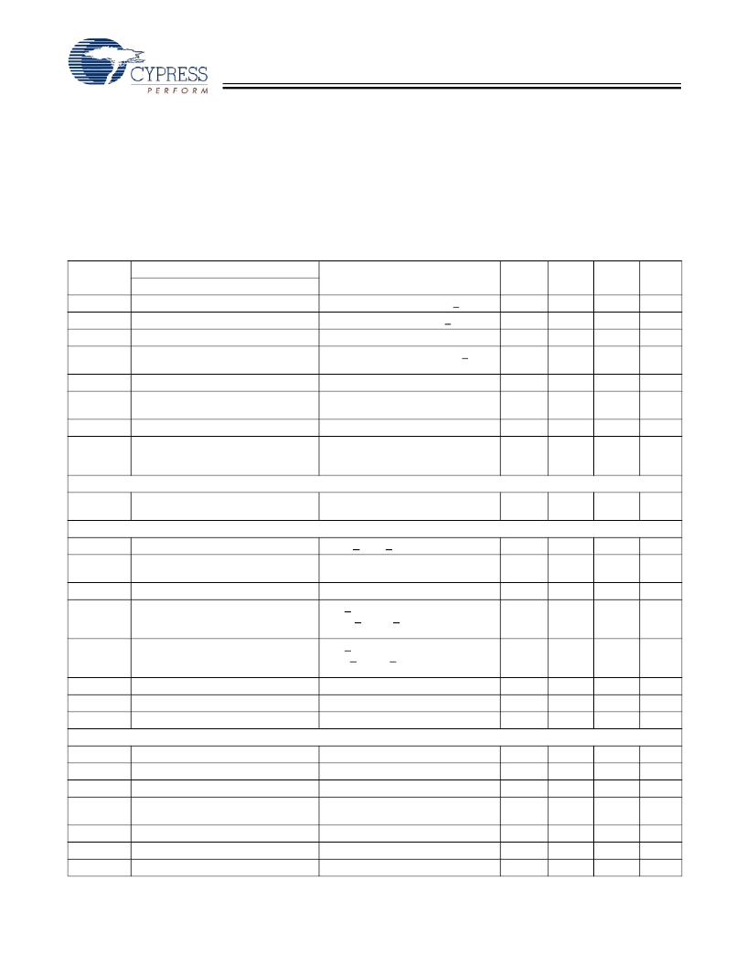
25.0
Absolute Maximum Ratings
Storage Temperature ..................................–65°C to +150°C
Ambient Temperature with Power Applied ..... –0°C to +70°C
Supply Voltage on V
CC
Relative to V
SS
..........–0.5V to +7.0V
DC Input Voltage................................ –0.5V to + V
CC
+ 0.5V
DC Voltage Applied to Outputs in
High-Z State ...................................... –0.5V to + V
CC
+ 0.5V
Maximum Total Sink Output Current into Port 0
and 1 and Pins.............................................................70 mA
Maximum Total Source Output Current into GPIO Pins30 mA
Maximum On-chip Power Dissipation
on any GPIO Pin.........................................................50 mW
Power Dissipation ....................................................300 mW
Static Discharge Voltage .............................................2200V
Latch-up Current ...................................................... 200 mA
26.0
DC Characteristics
Parameter
V
CC1
V
CC2
V
CC3
V
CC4
Description
General
Conditions
Min.
4.0
4.35
4.35
4.75
Typical
Max.
5.5
5.25
5.25
5.5
Unit
V
V
V
V
Operating Voltage
Operating Voltage
Operating Voltage
Operating Voltage
No USB activity, CPU speed < 12 MHz
USB activity, CPU speed < 12 MHz
Flash programming
No USB activity, CPU speed < 24
MHz
Flash Programming
V
= 5.25V, no GPIO loading,
24 MHz
V
CC
= 5.0V, no GPIO loading, 6 MHz
Internal and External Oscillators,
Bandgap, Flash, CPU Clock, Timer
Clock, USB Clock all disabled
T
FP
I
CC1
Operating Temp
V
CC
Operating Supply Current
0
70
40
°C
mA
I
CC2
I
SB1
V
CC
Operating Supply Current
Standby Current
10
mA
μ
A
10
Low-voltage Detect
V
LVD
Low-voltage detect Trip Voltage
(8 programmable trip points)
3.3V Regulator
I
VREG
Max Regulator Output Current
I
KA
Keep Alive Current
2.681
4.872
V
4.35V < V
CC
< 5.5V
When regulator is disabled with
“keep alive” enable
Keep Alive bit set in VREGCR
V
> 4.35V, 0 < temp < 40°C,
25 mA < I
< 125 mA (3.3V ± 8%)
T = 0 to 70C
V
> 4.35V, 0 < temp < 40°C,
1 mA < I
< 25 mA (3.3V ± 4%)
T = 0 to 40C
125
20
mA
μ
A
V
KA
V
REG1
Keep Alive Voltage
V
REG
Output Voltage
2.35
3.0
3.8
3.6
V
V
V
REG2
V
REG
Output Voltage
3.15
3.45
V
C
LOAD
LN
REG
LD
REG
USB Interface
V
ON
V
OFF
V
DI
V
CM
Capacitive load on Vreg pin
Line Regulation
Load Regulation
1
2
1
μ
F
%/V
%/mA
0.04
Static Output High
Static Output Low
Differential Input Sensitivity
Differential Input Common Mode
Range
Single Ended Receiver Threshold
Transceiver Capacitance
Hi-Z State Data Line Leakage
15K ± 5% Ohm to V
SS
R
UP
is enabled
2.8
3.6
0.3
V
V
V
V
0.2
0.8
2.5
V
SE
C
IN
I
IO
0.8
2
20
10
V
pF
μ
A
0V < V
IN
< 3.3V
–10
相關(guān)PDF資料 |
PDF描述 |
|---|---|
| CY7C65640-LFXC | TetraHub High-speed USB Hub Controller |
| CY7C65640 | TetraHub High-speed USB Hub Controller |
| CY7C65640-LFC | TetraHub High-speed USB Hub Controller |
| CY4602 | TetraHub High-speed USB Hub Controller |
| CY7C65640A | TetraHub High-Speed USB Hub Controller(TetraHub高速USB Hub控制器) |
相關(guān)代理商/技術(shù)參數(shù) |
參數(shù)描述 |
|---|---|
| CY7C638334-LTXC | 制造商:Cypress Semiconductor 功能描述: |
| CY7C638335-LFXC | 制造商:Cypress Semiconductor 功能描述: |
| CY7C638335-LTXC | 制造商:Cypress Semiconductor 功能描述: |
| CY7C63833-LFXC | 功能描述:USB 接口集成電路 8K Flash 256 byte RAM COM RoHS:否 制造商:Cypress Semiconductor 產(chǎn)品:USB 2.0 數(shù)據(jù)速率: 接口類(lèi)型:SPI 工作電源電壓:3.15 V to 3.45 V 工作電源電流: 最大工作溫度:+ 85 C 安裝風(fēng)格:SMD/SMT 封裝 / 箱體:WLCSP-20 |
| CY7C63833-LTXC | 功能描述:USB 接口集成電路 USB Peripheral Cntrl 8K/256 32-QFN RoHS:否 制造商:Cypress Semiconductor 產(chǎn)品:USB 2.0 數(shù)據(jù)速率: 接口類(lèi)型:SPI 工作電源電壓:3.15 V to 3.45 V 工作電源電流: 最大工作溫度:+ 85 C 安裝風(fēng)格:SMD/SMT 封裝 / 箱體:WLCSP-20 |
發(fā)布緊急采購(gòu),3分鐘左右您將得到回復(fù)。