- 您現(xiàn)在的位置:買賣IC網(wǎng) > PDF目錄379091 > CY7C371i (Cypress Semiconductor Corp.) UltraLogic 32-Macrocell Flash CPLD(超邏輯的32 宏單元閃速 CPLD) PDF資料下載
參數(shù)資料
| 型號(hào): | CY7C371i |
| 廠商: | Cypress Semiconductor Corp. |
| 英文描述: | UltraLogic 32-Macrocell Flash CPLD(超邏輯的32 宏單元閃速 CPLD) |
| 中文描述: | UltraLogic 32宏單元CPLD的閃光(超邏輯的32個(gè)宏單元閃速的CPLD) |
| 文件頁(yè)數(shù): | 2/11頁(yè) |
| 文件大?。?/td> | 190K |
| 代理商: | CY7C371I |
CY7C371i
2
Functional Description
(continued)
Finally, the CY7C371i features a very simple timing model.
Unlike other high-density CPLD architectures, there are no
hidden speed delays such as fanout effects, interconnect de-
lays, or expander delays. Regardless of the number of re-
sources used or the type of application, the timing parameters
on the CY7C371i remain the same.
Logic Block
The number of logic blocks distinguishes the members of the
F
LASH
370i family. The CY7C371i includes two logic blocks.
Each logic block is constructed of a product term array, a prod-
uct term allocator, and 16 macrocells.
Product Term Array
The product term array in the F
LASH
370i logic block includes
36 inputs from the PIM and outputs 86 product terms to the
product term allocator. The 36 inputs from the PIM are avail-
able in both positive and negative polarity, making the overall
array size 72 x 86. This large array in each logic block allows
for very complex functions to be implemented in a single pass
through the device.
Product Term Allocator
The product term allocator is a dynamic, configurable resource
that shifts product terms to macrocells that require them. Any
number of product terms between 0 and 16 inclusive can be
assigned to any of the logic block macrocells (this is called
product term steering). Furthermore, product terms can be
shared among multiple macrocells. This means that product
terms that are common to more than one output can be imple-
mented in a single product term. Product term steering and
product term sharing help to increase the effective density of
the F
LASH
370i CPLDs. Note that product term allocation is
handled by software and is invisible to the user.
I/O Macrocell
Each of the macrocells on the CY7C371i has a separate as-
sociated I/O pin. The input to the macrocell is the sum of be-
tween 0 and 16 product terms from the product term allocator.
The macrocell includes a register that can be optionally by-
passed. It also has polarity control, and two global clocks to
trigger the register. The macrocell also features a separate
feedback path to the PIM so that the register can be buried if
the I/O pin is used as an input.
Programmable Interconnect Matrix
The Programmable Interconnect Matrix (PIM) connects the
two logic blocks on the CY7C371i to the inputs and to each
other. All inputs (including feedbacks) travel through the PIM.
There is no speed penalty incurred by signals traversing the
PIM.
Programming
For an overview of ISR programming, refer to the F
LASH
370i
Family data sheet and for ISR cable and software specifica-
tions, refer to ISR data sheets. For a detailed description of
ISR capabilities, refer to the Cypress application note,
“
An In-
troduction to In System Reprogramming with F
LASH
370i.
”
PCI Compliance
The F
LASH
370i family of CMOS CPLDs are fully compliant with
the PCI Local Bus Specification published by the PCI Special
Interest Group. The simple and predictable timing model of
F
LASH
370i ensures compliance with the PCI AC specifications
independent of the design. On the other hand, in CPLD and
FPGA architectures without simple and predictable timing, PCI
compliance is dependent upon routing and product term dis-
tribution.
3.3V or 5.0V I/O operation
The F
LASH
370i family can be configured to operate in both 3.3V
and 5.0V systems. All devices have two sets of V
CC
pins: one
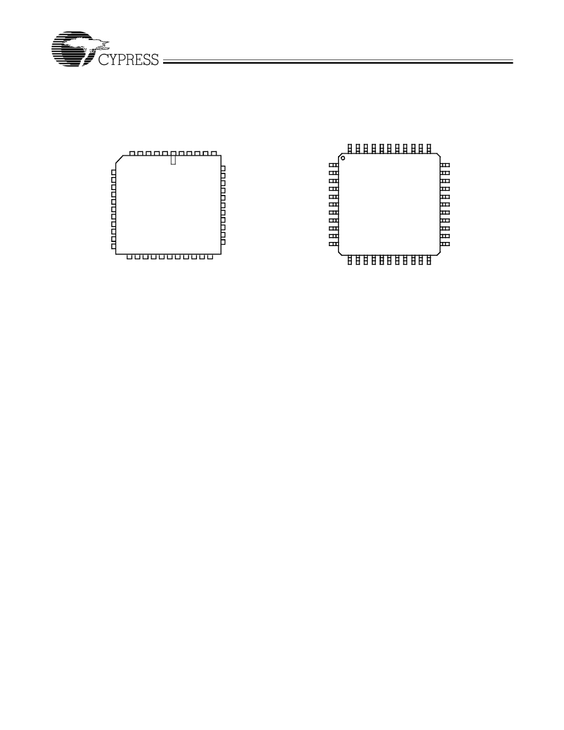
Pin Configurations
7c371i
–
2
I/O
27
/SDI
I/O
26
I/O
25
I/O
24
CLK
1
/I
4
GND
I
3
I
2
I/O
23
I/O
22
I/O
21
I/O
5
/SCLK
I/O
6
I/O
7
I
0
ISR
EN
GND
CLK
0
/I
1
I/O
8
I/O
9
I/O
10
I/O
11
G
I2
I
G
V
VC
I
I
I
I
I
I
I
I
I1
I1
I1
I1
I1
I1
I1
I1
6 5
3
4
2
8
9
10
11
12
7
1 44
18
15
16
17
14
13
19 20
22
21
23 24
27
26
28
25
31
30
29
32
33
34
39
38
37
36
35
43 42
40
41
I
G
V
I
I
I
I
I
I
I
I
I/O
27
/SDI
I/O
26
I/O
25
I/O
24
CLK
1
/I
4
GND
I
3
I
2
I/O
23
I/O
22
I/O
21
G
I2
VC
I1
I1
I1
I1
I1
I1
I/O
5
/SCLK
I/O
6
I/O
7
I
0
GND
CLK
0
/I
1
I/O
8
I/O
9
I/O
10
I/O
11
8
9
10
11
7
3
4
5
6
2
1
18 19 20
22
21
13 14 15
17
16
12
31
30
29
28
32
33
26
25
24
23
27
44 43 42
40
41
39 38 37
35
36
34
7c371i
–
3
PLCC
TopView
TQFP
TopView
/
/
I1
I1
ISR
EN
相關(guān)PDF資料 |
PDF描述 |
|---|---|
| CY7C372i | UltraLogic 64-Macrocell Flash CPLD(超邏輯的64 宏單元 閃速 CPLD) |
| CY7C372 | UltraLogic 64-Macrocell Flash CPLD(超邏輯的64-宏單元閃速CPLD) |
| CY7C373i | UltraLogic 64-Macrocell Flash CPLD(超邏輯的64 宏單元閃速 CPLD) |
| CY7C374I-66JC | UltraLogic 128-Macrocell Flash CPLD |
| CY7C374I-83YMB | UltraLogic 128-Macrocell Flash CPLD |
相關(guān)代理商/技術(shù)參數(shù) |
參數(shù)描述 |
|---|---|
| CY7C371I-110AC | 制造商:Cypress Semiconductor 功能描述:CPLD FLASH370i Family 800 Gates 32 Macro Cells 111MHz 5V 44-Pin TQFP 制造商:Cypress Semiconductor 功能描述:CPLD FLASH370i Family 800 Gates 32 Macro Cells 111MHz CMOS Technology 5V 44-Pin TQFP |
| CY7C371I-110AI | 制造商:Rochester Electronics LLC 功能描述:- Bulk 制造商:Cypress Semiconductor 功能描述: |
| CY7C371I-66AC | 制造商:Cypress Semiconductor 功能描述:CPLD FLASH370i Family 800 Gates 32 Macro Cells 66.6MHz CMOS Technology 5V 44-Pin TQFP 制造商:Cypress Semiconductor 功能描述:CPLD FLASH370i Family 800 Gates 32 Macro Cells 66.6MHz 5V 44-Pin TQFP |
| CY7C371I-66JC | 制造商:Cypress Semiconductor 功能描述: |
| CY7C371I-83JC | 制造商:Cypress Semiconductor 功能描述:CPLD FLASH370i Family 800 Gates 32 Macro Cells 83.3MHz CMOS Technology 5V 44-Pin PLCC |
發(fā)布緊急采購(gòu),3分鐘左右您將得到回復(fù)。