- 您現(xiàn)在的位置:買賣IC網(wǎng) > PDF目錄379077 > CY7C1475V25-100BGXI (CYPRESS SEMICONDUCTOR CORP) 72-Mbit (2M x 36/4M x 18/1M x 72) Flow-Through SRAM with NoBL⑩ Architecture PDF資料下載
參數(shù)資料
| 型號(hào): | CY7C1475V25-100BGXI |
| 廠商: | CYPRESS SEMICONDUCTOR CORP |
| 元件分類: | DRAM |
| 英文描述: | 72-Mbit (2M x 36/4M x 18/1M x 72) Flow-Through SRAM with NoBL⑩ Architecture |
| 中文描述: | 1M X 72 ZBT SRAM, 8.5 ns, PBGA209 |
| 封裝: | 14 X 22 MM, 1.76 MM HEIGHT, LEAD FREE, FBGA-209 |
| 文件頁數(shù): | 17/32頁 |
| 文件大小: | 928K |
| 代理商: | CY7C1475V25-100BGXI |
第1頁第2頁第3頁第4頁第5頁第6頁第7頁第8頁第9頁第10頁第11頁第12頁第13頁第14頁第15頁第16頁當(dāng)前第17頁第18頁第19頁第20頁第21頁第22頁第23頁第24頁第25頁第26頁第27頁第28頁第29頁第30頁第31頁第32頁
CY7C1471V25
CY7C1473V25
CY7C1475V25
Document #: 38-05287 Rev. *I
Page 17 of 32
1.8V TAP AC Test Conditions
Input pulse levels.....................................0.2V to V
DDQ
– 0.2
Input rise and fall time..................................................... 1 ns
Input timing reference levels...........................................0.9V
Output reference levels...................................................0.9V
Test load termination supply voltage...............................0.9V
2.5V TAP AC Test Conditions
Input pulse levels.................................................V
SS
to 2.5V
Input rise and fall time .....................................................1 ns
Input timing reference levels.........................................1.25V
Output reference levels ................................................1.25V
Test load termination supply voltage ............................1.25V
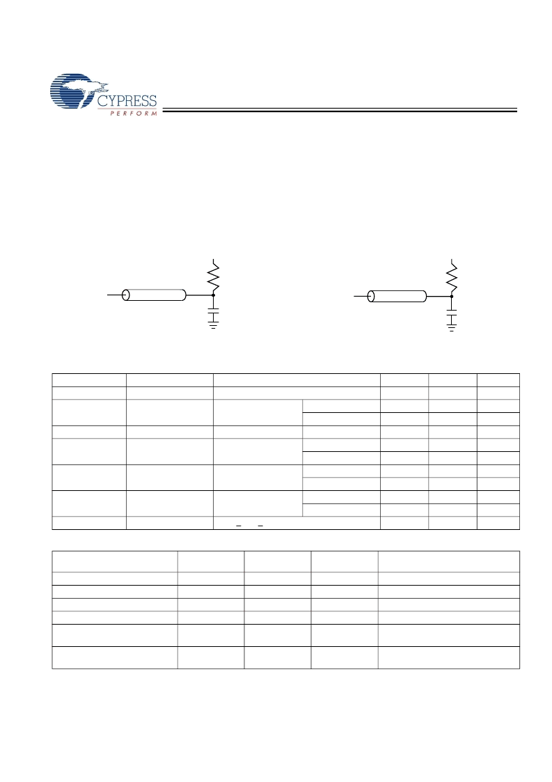
1.8V TAP AC Output Load Equivalent
TDO
0.9V
20pF
Z = 50
50
2.5V TAP AC Output Load Equivalent
TDO
1.25V
20pF
Z = 50
50
TAP DC Electrical Characteristics And Operating Conditions
(0°C < T
A
< +70°C; V
DD
= 2.375 to 2.625 unless otherwise noted)
[12]
Parameter
Description
V
OH1
Output HIGH Voltage
V
OH2
Output HIGH Voltage
Test Conditions
Min.
2.0
2.1
1.6
Max.
Unit
V
V
V
V
V
V
V
V
V
V
μA
I
OH
= –1.0 mA, V
DDQ
= 2.5V
I
OH
= –100 μA
V
DDQ
= 2.5V
V
DDQ
= 1.8V
V
DDQ
= 2.5V
V
DDQ
= 2.5V
V
DDQ
= 1.8V
V
DDQ
= 2.5V
V
DDQ
= 1.8V
V
DDQ
= 2.5V
V
DDQ
= 1.8V
V
OL1
V
OL2
Output LOW Voltage
Output LOW Voltage
I
OL
= 1.0 mA
I
OL
= 100 μA
0.4
0.2
0.2
V
IH
Input HIGH Voltage
1.7
1.26
–0.3
–0.3
–5
V
DD
+ 0.3
V
DD
+ 0.3
0.7
0.36
5
V
IL
Input LOW Voltage
I
X
Input Load Current
GND < V
IN
< V
DDQ
Identification Register Definitions
Instruction Field
CY7C1471V25
(2MX36)
000
01011
001001
100100
00000110100
CY7C1473V25
(4MX18)
000
01011
001001
010100
00000110100
CY7C1475V25
(1MX72)
000
01011
001001
110100
00000110100
Description
Revision Number (31:29)
Device Depth (28:24)
Architecture/Memory Type(23:18)
Bus Width/Density(17:12)
Cypress JEDEC ID Code (11:1)
Describes the version number
Reserved for internal use
Defines memory type and architecture
Defines width and density
Allows unique identification of SRAM
vendor
Indicates the presence of an ID
register
ID Register Presence Indicator (0)
1
1
1
Note
12.All voltages refer to V
SS
(GND).
相關(guān)PDF資料 |
PDF描述 |
|---|---|
| CY7C1475V25-133BGI | 72-Mbit (2M x 36/4M x 18/1M x 72) Flow-Through SRAM with NoBL⑩ Architecture |
| CY7C1475V25-133BGXI | 72-Mbit (2M x 36/4M x 18/1M x 72) Flow-Through SRAM with NoBL⑩ Architecture |
| CY7C1475V25 | 72-Mbit (2M x 36/4M x 18/1M x 72) Flow-Through SRAM with NoBL Architecture(帶NoBL結(jié)構(gòu)的72-Mbit (2M x 36/4M x 18/1M x 72) Flow-Through SRAM) |
| CY7C1473V25 | 72-Mbit (2M x 36/4M x 18/1M x 72) Flow-Through SRAM with NoBL Architecture(帶NoBL結(jié)構(gòu)的72-Mbit (2M x 36/4M x 18/1M x 72) Flow-Through SRAM) |
| CY7C1475V33 | 72-Mbit (2M x 36/4M x 18/1M x 72) Flow-Through SRAM with NoBL Architecture(帶NoBL結(jié)構(gòu)的72-Mbit (2M x 36/4M x 18/1M x 72) Flow-Through SRAM) |
相關(guān)代理商/技術(shù)參數(shù) |
參數(shù)描述 |
|---|---|
| CY7C1475V33-100AXC | 制造商:Cypress Semiconductor 功能描述:72MB (1MBX72) NOBL FLOW-THRU, 3.3V CORE, 2.5/3.3V I/O - Bulk |
| CY7C1475V33-100BGC | 制造商:Cypress Semiconductor 功能描述:SRAM SYNC SGL 3.3V 72MBIT 1MX72 8.5NS 209FBGA - Bulk |
| CY7C1475V33-133BGC | 制造商:Cypress Semiconductor 功能描述:SRAM SYNC OCTAL 3.3V 72MBIT 1MX72 6.5NS 209FBGA - Bulk |
| CY7C14802BC | 制造商:Cypress Semiconductor 功能描述: |
| CY7C14802XC | 制造商:Cypress Semiconductor 功能描述: |
發(fā)布緊急采購(gòu),3分鐘左右您將得到回復(fù)。