- 您現(xiàn)在的位置:買賣IC網 > PDF目錄379067 > CY7C1370D-250AXI (CYPRESS SEMICONDUCTOR CORP) 18-Mbit (512K X 36/1M X 18) Pipelined SRAM with NoBL Architecture PDF資料下載
參數(shù)資料
| 型號: | CY7C1370D-250AXI |
| 廠商: | CYPRESS SEMICONDUCTOR CORP |
| 元件分類: | DRAM |
| 英文描述: | 18-Mbit (512K X 36/1M X 18) Pipelined SRAM with NoBL Architecture |
| 中文描述: | 512K X 36 ZBT SRAM, 2.6 ns, PQFP100 |
| 封裝: | (14 X 20 X 1.4) MM, LEAD FREE, PLASTIC, TQFP-100 |
| 文件頁數(shù): | 15/30頁 |
| 文件大小: | 344K |
| 代理商: | CY7C1370D-250AXI |
第1頁第2頁第3頁第4頁第5頁第6頁第7頁第8頁第9頁第10頁第11頁第12頁第13頁第14頁當前第15頁第16頁第17頁第18頁第19頁第20頁第21頁第22頁第23頁第24頁第25頁第26頁第27頁第28頁第29頁第30頁
PRELIMINARY
CY7C1370D
CY7C1372D
Document #: 38-05555 Rev. *A
Page 15 of 30
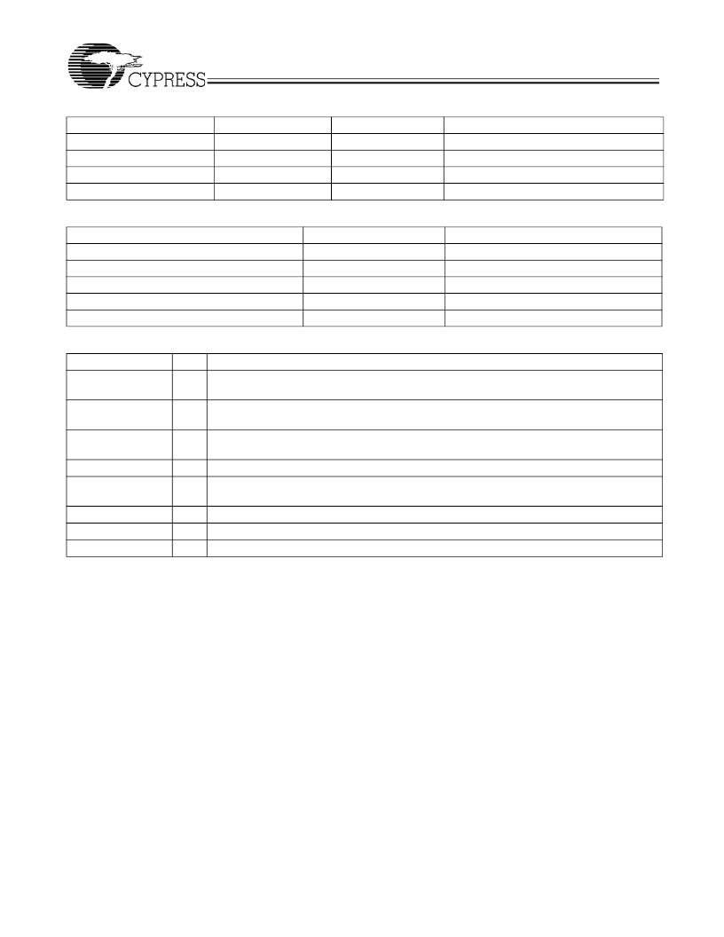
Identification Register Definitions
Instruction Field
Revision Number (31:29)
Cypress Device ID (28:12)
[12]
Cypress JEDEC ID (11:1)
ID Register Presence (0)
CY7C1370D
000
01011001000100101
00000110100
1
CY7C1372D
000
01011001000010101 Reserved for future use.
00000110100
Allows unique identification of SRAM vendor.
1
Indicate the presence of an ID register.
Description
Reserved for version number.
Scan Register Sizes
Register Name
Bit Size (x18)
3
1
32
85
89
Bit Size (x36)
3
1
32
85
89
Instruction
Bypass
ID
Boundary Scan Order (119-ball BGA package)
Boundary Scan Order (165-ball fBGA package)
Identification Codes
Instruction
EXTEST
Code
000
Description
Captures I/O ring contents. Places the boundary scan register between TDI and TDO.
Forces all SRAM outputs to High-Z state.
Loads the ID register with the vendor ID code and places the register between TDI and TDO.
This operation does not affect SRAM operations.
Captures I/O ring contents. Places the boundary scan register between TDI and TDO.
Forces all SRAM output drivers to a High-Z state.
Do Not Use: This instruction is reserved for future use.
Captures I/O ring contents. Places the boundary scan register between TDI and TDO.
Does not affect SRAM operation.
Do Not Use: This instruction is reserved for future use.
Do Not Use: This instruction is reserved for future use.
Places the bypass register between TDI and TDO. This operation does not affect SRAM operations.
IDCODE
001
SAMPLE Z
010
RESERVED
SAMPLE/PRELOAD
011
100
RESERVED
RESERVED
BYPASS
101
110
111
Note:
12.Bit #24 is “1” in the Register Definitions for both 2.5v and 3.3v versions of this device.
相關PDF資料 |
PDF描述 |
|---|---|
| CY7C1370D-250BGC | 18-Mbit (512K X 36/1M X 18) Pipelined SRAM with NoBL Architecture |
| CY7C1370D-250BGI | 18-Mbit (512K X 36/1M X 18) Pipelined SRAM with NoBL Architecture |
| CY7C1370D-250BZC | 18-Mbit (512K X 36/1M X 18) Pipelined SRAM with NoBL Architecture |
| CY7C1370D-250BZI | 18-Mbit (512K X 36/1M X 18) Pipelined SRAM with NoBL Architecture |
| CY7C1372D | 18-Mbit (512K X 36/1M X 18) Pipelined SRAM with NoBL Architecture |
相關代理商/技術參數(shù) |
參數(shù)描述 |
|---|---|
| CY7C1370D-250BZC | 制造商:Cypress Semiconductor 功能描述:SRAM SYNC QUAD 3.3V 18MBIT 512KX36 2.6NS 165FBGA - Bulk |
| CY7C1370DV25-167 | 制造商:Cypress Semiconductor 功能描述: |
| CY7C1370DV25-167AXC | 功能描述:靜態(tài)隨機存取存儲器 512Kx36 2.5V NoBL Sync PL 靜態(tài)隨機存取存儲器 COM RoHS:否 制造商:Cypress Semiconductor 存儲容量:16 Mbit 組織:1 M x 16 訪問時間:55 ns 電源電壓-最大:3.6 V 電源電壓-最小:2.2 V 最大工作電流:22 uA 最大工作溫度:+ 85 C 最小工作溫度:- 40 C 安裝風格:SMD/SMT 封裝 / 箱體:TSOP-48 封裝:Tray |
| CY7C1370DV25-167AXCT | 功能描述:靜態(tài)隨機存取存儲器 512Kx36 2.5V NoBL Sync PL 靜態(tài)隨機存取存儲器 COM RoHS:否 制造商:Cypress Semiconductor 存儲容量:16 Mbit 組織:1 M x 16 訪問時間:55 ns 電源電壓-最大:3.6 V 電源電壓-最小:2.2 V 最大工作電流:22 uA 最大工作溫度:+ 85 C 最小工作溫度:- 40 C 安裝風格:SMD/SMT 封裝 / 箱體:TSOP-48 封裝:Tray |
| CY7C1370DV25-167AXI | 功能描述:靜態(tài)隨機存取存儲器 512Kx36 2.5V NoBL Sync PL 靜態(tài)隨機存取存儲器 IND RoHS:否 制造商:Cypress Semiconductor 存儲容量:16 Mbit 組織:1 M x 16 訪問時間:55 ns 電源電壓-最大:3.6 V 電源電壓-最小:2.2 V 最大工作電流:22 uA 最大工作溫度:+ 85 C 最小工作溫度:- 40 C 安裝風格:SMD/SMT 封裝 / 箱體:TSOP-48 封裝:Tray |
發(fā)布緊急采購,3分鐘左右您將得到回復。