- 您現(xiàn)在的位置:買賣IC網(wǎng) > PDF目錄379008 > CY2CC1910SI (CYPRESS SEMICONDUCTOR CORP) 1:10 Clock Fanout Buffer with Output Enable PDF資料下載
參數(shù)資料
| 型號: | CY2CC1910SI |
| 廠商: | CYPRESS SEMICONDUCTOR CORP |
| 元件分類: | 時鐘及定時 |
| 英文描述: | 1:10 Clock Fanout Buffer with Output Enable |
| 中文描述: | LOW SKEW CLOCK DRIVER, 10 TRUE OUTPUT(S), 0 INVERTED OUTPUT(S), PDSO24 |
| 封裝: | 0.300 INCH, SOIC-24 |
| 文件頁數(shù): | 4/8頁 |
| 文件大?。?/td> | 129K |
| 代理商: | CY2CC1910SI |
COMLINK
SERIES
CY2CC1910
Document #: 38-07347 Rev. *B
Page 4 of 8
AC Switching Characteristics
@ 3.3V V
DD
= 3.3V ± 5%, Temperature =
–
40
°
C to +85
°
C
Parameter
t
PLH
Propagation Delay
–
Low to High
t
PHL
Propagation Delay
–
High to Low
t
R
Output Rise Time
t
F
Output Fall Time
t
SK(0)
Output Skew: Skew between outputs of the same package (in phase)
t
SK(p)
Pulse Skew: Skew between opposite transitions of the same output (t
PHL
–
t
PLH
).
t
SK(t)
Package Skew: Skew between outputs of different packages at the same
power supply Voltage, temperature and package type.
Parameter Measurement Information:
V
DD
@ 3.3V
–
2.5V
Notes:
4.
5.
6.
7.
C
includes probe and jig capacitance.
All input pulses are supplied by generators having the following characteristics: PRR < 100 MHz, Z
0
= 50
, t
R
< 2.5 nS, t
F
< 2.5 nS.
The outputs are measured one at a time with one transition per measurement.
T
PLH
and T
PHL
are the same as t
pd
.
Description
Min.
1.5
1.5
Typ.
2.7
2.7
0.8
0.8
Max.
3.5
3.5
Unit
nS
nS
V/nS
V/nS
nS
nS
Figure 3
Figure 10
Figure 9
0.2
0.2
Figure 11
0.4
nS
AC Switching Characteristics
@ 2.5V V
DD
= 2.5V ± 5%, Temperature =
–
40
°
C to +85
°
C
Parameter
t
PLH
Propagation Delay
–
Low to High
t
PHL
Propagation Delay
–
High to Low
t
R
Output Rise Time
t
F
Output Fall Time
t
SK(0)
Output Skew: Skew between outputs of the same package (in phase)
t
SK(p)
Pulse Skew: Skew between opposite transitions of the same output (t
PHL
–
t
PLH
).
t
SK(t)
Package Skew: Skew between outputs of different packages at the
same power supply Voltage, temperature and package type.
Description
Min.
1.5
1.5
Typ.
2.7
2.7
0.8
0.8
Max.
3.5
3.5
Unit
nS
nS
V/nS
V/nS
nS
nS
Figure 3
Figure 10
Figure 9
0.2
0.2
Figure 11
0.4
nS
AC Switching Characteristics
@ 1.8V V
DD
= 1.8V ± 5%, Temperature =
–
40
°
C to +85
°
C
Parameter
t
PLH
Propagation Delay
–
Low to High
t
PHL
Propagation Delay
–
High to Low
t
R
Output Rise Time 20
–
80%
t
F
Output Fall Time 20
–
80%
t
SK(0)
Output Skew: Skew between outputs of the same package (in phase)
t
SK(p)
Pulse Skew: Skew between opposite transitions of the same output (t
PHL
–
t
PLH
).
t
SK(t)
Package Skew: Skew between outputs of different packages at the same
power supply Voltage, temperature and package type.
Description
Min.
1.5
1.5
0.2
0.2
Typ.
2.7
2.7
Max.
3.5
3.5
1.5
1.5
0.2
0.2
Unit
nS
nS
nS
nS
nS
nS
Figure 7
Figure 10
Figure 9
Figure 11
0.4
nS
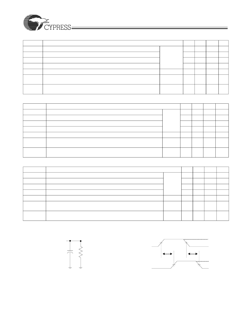
From Output
Under Test
C
L
= 50 pF
500 ohm
Figure 2. Load Circuit
[4,5,6]
VDD/2
t
PLH
t
PHL
V
OH
V
OL
0 V
Input
Output
VDD/2
VDD/2
VDD/2
0.8VDD
Figure 3. Voltage Waveforms Propagation Delay Times
[7]
相關PDF資料 |
PDF描述 |
|---|---|
| CY2CC1910SIT | 1:10 Clock Fanout Buffer with Output Enable |
| CY2DP814SC | 1:4 Clock Fanout Buffer |
| CY2DP814ZC | DB37 INTERFACE DATA CBL DB37 Male - DB37 Female |
| CY2DP814ZCT | DB37 INTERFACE DATA CBL DB37 Male - DB37 Female |
| CY2DP814 | 1:4 Clock Fanout Buffer |
相關代理商/技術參數(shù) |
參數(shù)描述 |
|---|---|
| CY2CC1910SIT | 制造商:CYPRESS 制造商全稱:Cypress Semiconductor 功能描述:1:10 Clock Fanout Buffer with Output Enable |
| CY2CC810 | 制造商:CYPRESS 制造商全稱:Cypress Semiconductor 功能描述:1:10 Clock Fanout Buffer |
| CY2CC810_06 | 制造商:CYPRESS 制造商全稱:Cypress Semiconductor 功能描述:1:10 Clock Fanout Buffer |
| CY2CC8100I | 制造商:Cypress Semiconductor 功能描述: |
| CY2CC8100XC-1 | 制造商:Cypress Semiconductor 功能描述: |
發(fā)布緊急采購,3分鐘左右您將得到回復。