- 您現(xiàn)在的位置:買賣IC網(wǎng) > PDF目錄378482 > CY28326 (Cypress Semiconductor Corp.) FTG for VIA PT880 Serial Chipset PDF資料下載
參數(shù)資料
| 型號: | CY28326 |
| 廠商: | Cypress Semiconductor Corp. |
| 英文描述: | FTG for VIA PT880 Serial Chipset |
| 中文描述: | FTG的威盛PT880系列芯片組 |
| 文件頁數(shù): | 18/23頁 |
| 文件大小: | 288K |
| 代理商: | CY28326 |
CY28326
Document #: 38-07616 Rev. *A
Page 18 of 23
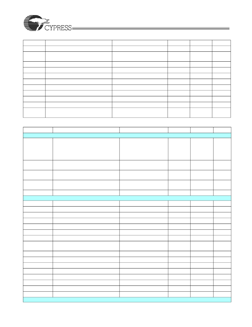
V
IH
I
IL
Input High Voltage
Input Leakage Current
2.0
–5
V
DD
+0. 5
5
V
μA
except Pull-ups or Pull downs
0 < V
IN
< V
DD
I
OL
= 1 mA
I
OH
= –1 mA
V
OL
V
OH
I
OZ
C
IN
C
OUT
L
IN
V
XIH
V
XIL
I
DD
Output Low Voltage
Output High Voltage
High-Impedance Output Current
Input Pin Capacitance
Output Pin Capacitance
Pin Inductance
Xin High Voltage
Xin Low Voltage
Dynamic Supply Current
–
0.4
–
10
5
6
7
V
DD
0.3V
DD
350
V
V
μA
pF
pF
nH
V
V
mA
2.4
–10
2
3
–
0.7V
DD
0
–
At 200 MHz and all outputs
loaded per
Table 8
and
Figure 15
AC Electrical Specifications
Parameter
Crystal
T
DC
Description
Condition
Min.
Max.
Unit
XIN Duty Cycle
The device will operate
reliably with input duty cycles
up to 30/70 but the REF clock
duty cycle will not be within
specification
When Xin is driven from an
external clock source
Measured between 0.3V
DD
and 0.7V
DD
As an average over 1
μ
s
duration
Over 150 ms
47.5
52.5
%
T
PERIOD
XIN period
69.841
71.0
ns
T
R
/ T
F
XIN Rise and Fall Times
–
10.0
ns
T
CCJ
XIN Cycle to Cycle Jitter
–
500
ps
L
ACC
CPU at 0.7V
T
DC
T
PERIOD
T
PERIOD
T
PERIOD
T
PERIOD
T
SKEW
T
CCJ
T
R
/ T
F
Long Term Accuracy
300
ppm
CPUT and CPUC Duty Cycle
100 MHz CPUT and CPUC Period
133 MHz CPUT and CPUC Period
166 MHz CPUT and CPUC Period
200 MHz CPUT and CPUC Period
Any CPUT/C to CPUT/C Clock Skew
CPUT/C Cycle to Cycle Jitter
CPUT and CPUC Rise and Fall Times
Measured at crossing point V
OX
Measured at crossing point V
OX
Measured at crossing point V
OX
Measured at crossing point V
OX
Measured at crossing point V
OX
Measured at crossing point V
OX
Measured at crossing point V
OX
Measured from Vol = 0.175 to
Voh = 0.525V
38
62
%
ns
ns
ns
ns
ps
ps
9.9970
7.4978
5.9982
4.9985
–
–
10.003
7.5023
6.0018
5.0015
±110
250
175
1300
ps
T
R
T
F
V
HIGH
V
LOW
V
OX
V
OVS
V
UDS
V
RB
AGP
Rise Time Variation
Fall Time Variation
Voltage High
Voltage Low
Crossing Point Voltage at 0.7V Swing
Maximum Overshoot Voltage
Minimum Undershoot Voltage
Ring Back Voltage
–
–
550
550
850
–
550
ps
ps
mv
mv
mv
V
V
V
Math averages
Figure 15
Math averages
Figure 15
660
–150
200
–
–0.3
–
V
HIGH
+ 0.3
–
0.2
See
Figure 15
. Measure SE
DC Electrical Specifications
Parameter
Description
Condition
Min.
Max.
Unit
相關(guān)PDF資料 |
PDF描述 |
|---|---|
| CY28326OC | FTG for VIA PT880 Serial Chipset |
| CY28326OCT | FTG for VIA PT880 Serial Chipset |
| CY28326OXC | Single Pole Normally Open: 1-Form-A |
| CY28326OXCT | Single Pole Normally Open: 1-Form-A |
| CY28341-2 | Universal Clock Chip for VIA P4M/KT/KM400 DDR Systems |
相關(guān)代理商/技術(shù)參數(shù) |
參數(shù)描述 |
|---|---|
| CY28326OC | 制造商:CYPRESS 制造商全稱:Cypress Semiconductor 功能描述:FTG for VIA PT880 Serial Chipset |
| CY28326OCT | 制造商:CYPRESS 制造商全稱:Cypress Semiconductor 功能描述:FTG for VIA PT880 Serial Chipset |
| CY28326OXC | 制造商:Rochester Electronics LLC 功能描述:- Bulk |
| CY28326OXCT | 制造商:CYPRESS 制造商全稱:Cypress Semiconductor 功能描述:FTG for VIA PT880 Serial Chipset |
| CY28326SPC | 制造商:Cypress Semiconductor 功能描述: |
發(fā)布緊急采購,3分鐘左右您將得到回復(fù)。