- 您現(xiàn)在的位置:買賣IC網(wǎng) > PDF目錄378471 > CXD3021 (Sony Corporation) CD Digital Signal Processor with Built-in Digital Servo and DAC PDF資料下載
參數(shù)資料
| 型號: | CXD3021 |
| 廠商: | Sony Corporation |
| 元件分類: | 數(shù)字信號處理 |
| 英文描述: | CD Digital Signal Processor with Built-in Digital Servo and DAC |
| 中文描述: | CD數(shù)字信號處理器,具有內(nèi)置數(shù)字伺服和DAC |
| 文件頁數(shù): | 112/161頁 |
| 文件大小: | 1311K |
| 代理商: | CXD3021 |
第1頁第2頁第3頁第4頁第5頁第6頁第7頁第8頁第9頁第10頁第11頁第12頁第13頁第14頁第15頁第16頁第17頁第18頁第19頁第20頁第21頁第22頁第23頁第24頁第25頁第26頁第27頁第28頁第29頁第30頁第31頁第32頁第33頁第34頁第35頁第36頁第37頁第38頁第39頁第40頁第41頁第42頁第43頁第44頁第45頁第46頁第47頁第48頁第49頁第50頁第51頁第52頁第53頁第54頁第55頁第56頁第57頁第58頁第59頁第60頁第61頁第62頁第63頁第64頁第65頁第66頁第67頁第68頁第69頁第70頁第71頁第72頁第73頁第74頁第75頁第76頁第77頁第78頁第79頁第80頁第81頁第82頁第83頁第84頁第85頁第86頁第87頁第88頁第89頁第90頁第91頁第92頁第93頁第94頁第95頁第96頁第97頁第98頁第99頁第100頁第101頁第102頁第103頁第104頁第105頁第106頁第107頁第108頁第109頁第110頁第111頁當(dāng)前第112頁第113頁第114頁第115頁第116頁第117頁第118頁第119頁第120頁第121頁第122頁第123頁第124頁第125頁第126頁第127頁第128頁第129頁第130頁第131頁第132頁第133頁第134頁第135頁第136頁第137頁第138頁第139頁第140頁第141頁第142頁第143頁第144頁第145頁第146頁第147頁第148頁第149頁第150頁第151頁第152頁第153頁第154頁第155頁第156頁第157頁第158頁第159頁第160頁第161頁
– 112 –
CXD3021R
§ 5-3. DC Offset Cancel [AVRG (Average) Measurement and Compensation] (See Fig. 5-3.)
The CXD3021R can measure the averages of RFDC, VC, FE and TE and compensate these signals using the
measurement results to control the servo effectively. This AVRG measurement and compensation is
necessary to initialize the CXD3021R, and is able to cancel the DC offset.
AVRG measurement takes the levels applied to the VC, FE, RFDC and TE pins as the digital average values
of 256 samples, and then loads these values into each AVRG register.
The AVRG measurement commands are VCLM, FLM, RFLM and TLM of $38.
Measurement is on when the respective command is set to 1.
AVRG measurement requires approximately 2.9ms to 5.8ms (when MCK = 128Fs) after the command is received.
The completion of AVRG measurement operation can be monitored by the SENS pin. (See Timing Chart 5-2.)
Monitoring requires that the upper 8 bits of the command register are 38 (H).
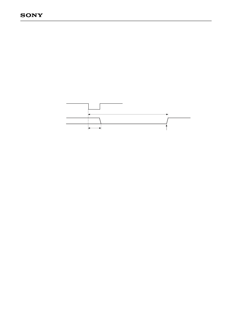
XLAT
SENS
(= XAVEBSY)
Max. 1μs
AVRG measurement completed
2.9 to 5.8ms
Timing Chart 5-2.
<Measurement>
VC AVRG: The VC DC offset (VC AVRG) which is the center voltage for the system is measured and used to
compensate the FE, TE and SE signals.
FE AVRG: The FE DC offset (FE AVRG) is measured and used to compensate the FE and FZC signals.
TE AVRG: The TE DC offset (TE AVRG) is measured and used to compensate the TE and SE signals.
RF AVRG: The RF DC offset (RF AVRG) is measured and used to compensate the RFDC signal.
<Compensation>
RFLC:
(RF signal – RF AVRG) is input to the RF In register.
"00" is input when the RF signal is lower than RF AVRG.
(TE signal – VC AVRG) is input to the TRK In register.
(TE signal – TE AVRG) is input to the TRK In register.
(FE signal – VC AVRG) is input to the FCS In register.
(FE signal – FE AVRG) is input to the FCS In register.
(FE signal – FE AVRG) is input to the FZC register.
TLC0:
TLC1:
VCLC:
FLC1:
FLC0:
Two methods of canceling the DC offset are assumed for the CXD3021R. These methods are shown in Figs.
5-3a and 5-3b.
An example of AVRG measurement and compensation commands is shown below.
$38 08 00
(RF AVRG measurement)
$38 20 00
(FE AVRG measurement)
$38 00 10
(TE AVRG measurement)
$38 14 0A
(Compensation on [RFLC, FLC0, FLC1, TLC1], corresponds to Fig. 5-3a.)
See the description of $38 for these commands.
相關(guān)PDF資料 |
PDF描述 |
|---|---|
| CXD3021R | Silver Mica Capacitor; Capacitance:25000pF; Capacitance Tolerance:+/- 1%; Series:CD42; Voltage Rating:500VDC; Capacitor Dielectric Material:Mica; Termination:Radial Leaded; Lead Pitch:27mm; Leaded Process Compatible:Yes RoHS Compliant: Yes |
| CXD3030 | System-on-a-Chip (SoC) Device Supports 48ⅴ Speed CD-ROM Drives |
| CXD3152R | Signal Processor LSI for Single-chip CCD B/W Camera |
| CXD3204R | IEEE1394 LSI for D-STB, D-VHS, and DTV |
| CXD3220 | IEEE1394 Link/Transaction Layer Controller LSI for SBP-2 |
相關(guān)代理商/技術(shù)參數(shù) |
參數(shù)描述 |
|---|---|
| CXD3021R | 制造商:SONY 制造商全稱:Sony Corporation 功能描述:CD Digital Signal Processor with Built-in Digital Servo and DAC |
| CXD3027 | 制造商:未知廠家 制造商全稱:未知廠家 功能描述:CD Audio Digital Signal-Processing LSI Device with On-Chip Digital Servo System Allows Listening without Sound Skipping |
| CXD3027R | 制造商:SONY 制造商全稱:Sony Corporation 功能描述:CD Digital Signal Processor with Built-in Digital Servo + Shock-Proof Memory Controller + Digital High & Bass Boost |
| CXD3027R-1 | 制造商:未知廠家 制造商全稱:未知廠家 功能描述:CD Audio Digital Signal-Processing LSI Device with On-Chip Digital Servo System Allows Listening without Sound Skipping |
| CXD3029R | 制造商:SONY 制造商全稱:Sony Corporation 功能描述:CD Digital Signal Processor with Built-in Digital Servo + Shock-proof Memory Controller + Digital High & Bass Boost |
發(fā)布緊急采購,3分鐘左右您將得到回復(fù)。