- 您現(xiàn)在的位置:買賣IC網(wǎng) > PDF目錄298969 > CS51220ED16 Analog IC PDF資料下載
參數(shù)資料
| 型號: | CS51220ED16 |
| 英文描述: | Analog IC |
| 中文描述: | 模擬IC |
| 文件頁數(shù): | 4/16頁 |
| 文件大小: | 184K |
| 代理商: | CS51220ED16 |
CS51220
http://onsemi.com
12
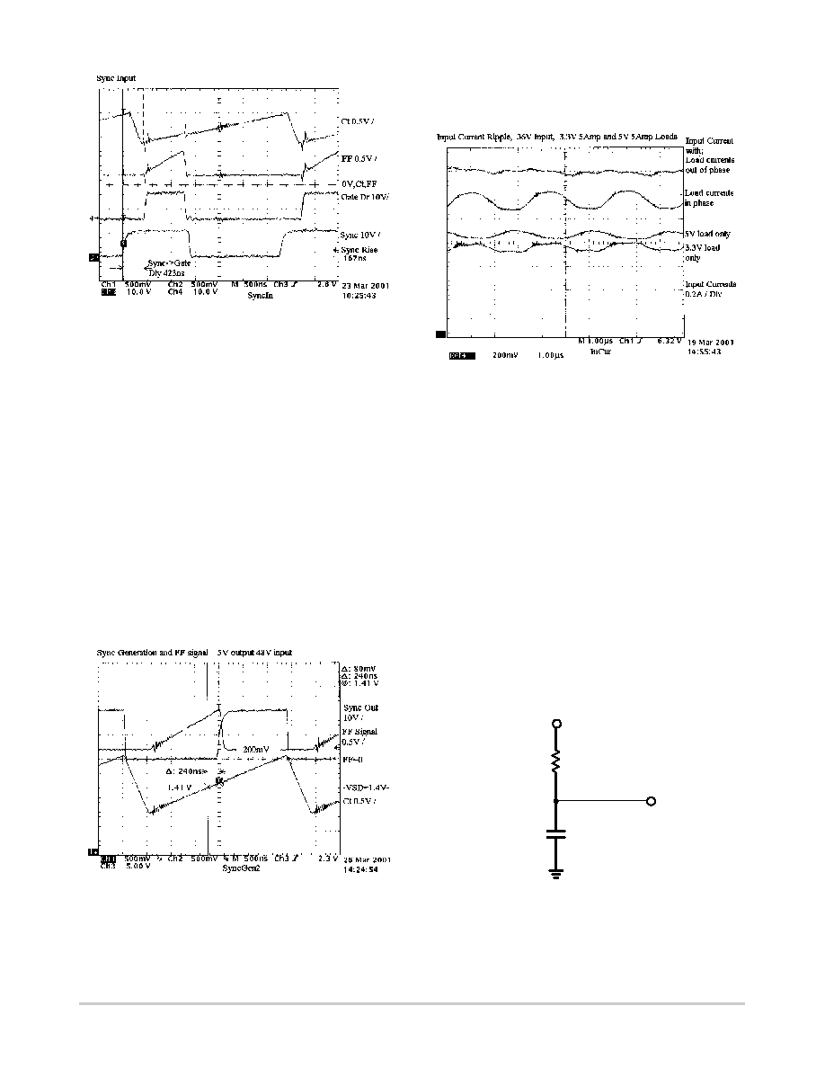
Figure 12. Synchronization Input Timing
Figure 12 shows the sync input from one CS51220 into
another. The delay between receiving the sync input and the
start of the next switching cycle is 423 ns. This delay must
be taken into account when establishing the total delay
between two regulators.
The SYNCO pin provides outgoing synchronization pulses
whose delay can be programmed by setting the voltage on the
VSD pin. The feature allows two converters to run at
interleaved phases. This implementation significantly
reduces the input ripple, and thus the number of input
capacitors. The phase delay is achieved by turning on
SYNCO output only after the CT pin voltage reaches the VSD
voltage. Therefore, the phase delay varies linearly with the
VSD voltage. The SYNCO output is reset during the falling
edge of the CT pin. For minimum phase delay (~ 240 ns), tie
the VSD pin to the ground. To entirely disable the SYNCO
output, connect the VSD pin to VREF.
The waveform in Figure 13 shows the CT ramp crossing
the VSD voltage set at 1.41 V.
Figure 13. Synchronization Output Timing
The delay from the point of crossing to the output of the
sync signal is 240 ns. The time for the sync out voltage is
measured at the +2.0 V level, which is the level that triggers
the next CS51220.
The desired effect on the input ripple is illustrated in
Figure 14. This is the input current for two power converters
operating from a 36 V line.
Figure 14. Input Current Ripple with
Different Overlap Conditions
The top waveform in Figure 14 is the input current with
the two supplies operating out of phase. The next down
shows the same supplies but with both conduction times
occurring simultaneously. The greatly increased ripple
current can be observed. The last two waveforms are the two
converters shown individually when operating out of phase.
DESIGN GUIDELINES
Program Volt–Second Clamp
Feed forward voltage mode control provides the
volt–second clamp which clamps the product of the line
voltage and switch on time. For the circuit shown in Figure 15,
the charging current of the CFF can be considered as a constant
current equal to VIN/RFF , provided VIN is much greater than
the FF pin voltage. Then the volt–second clamp provided by
CS51220 is given by
VINTON(MAX) + 1.0RFFCFF
VIN
RFF
CFF
FF Pin
Figure 15. An RC Network Provides Both
Volt–Second Clamp and Feed Forward Control
Select the time constant of the FF pin RC network to
provide desirable volt–second clamp.
相關(guān)PDF資料 |
PDF描述 |
|---|---|
| CS51411ED8 | SMPS Controller |
| CS51411EDR8 | SMPS Controller |
| CS51411GD8 | SMPS Controller |
| CS51411GDR8 | SMPS Controller |
| CS51412ED8 | SMPS Controller |
相關(guān)代理商/技術(shù)參數(shù) |
參數(shù)描述 |
|---|---|
| CS51220EDR16 | 功能描述:IC REG CTRLR DIV ISO PWM 16-SOIC RoHS:否 類別:集成電路 (IC) >> PMIC - 穩(wěn)壓器 - DC DC 切換控制器 系列:- 標(biāo)準(zhǔn)包裝:4,000 系列:- PWM 型:電壓模式 輸出數(shù):1 頻率 - 最大:1.5MHz 占空比:66.7% 電源電壓:4.75 V ~ 5.25 V 降壓:是 升壓:無 回掃:無 反相:無 倍增器:無 除法器:無 Cuk:無 隔離:無 工作溫度:-40°C ~ 85°C 封裝/外殼:40-VFQFN 裸露焊盤 包裝:帶卷 (TR) |
| CS51221 | 制造商:CHERRY 制造商全稱:CHERRY 功能描述:Enhanced Voltage Mode PWM Controller |
| CS51221/D | 制造商:未知廠家 制造商全稱:未知廠家 功能描述:Enhanced Voltage Mode PWM Controller |
| CS51221_09 | 制造商:ONSEMI 制造商全稱:ON Semiconductor 功能描述:Enhanced Voltage Mode PWM Controller |
| CS51221ED16 | 功能描述:電壓模式 PWM 控制器 Enhanced Current RoHS:否 制造商:Texas Instruments 輸出端數(shù)量:1 拓撲結(jié)構(gòu):Buck 輸出電壓:34 V 輸出電流: 開關(guān)頻率: 工作電源電壓:4.5 V to 5.5 V 電源電流:600 uA 最大工作溫度:+ 125 C 最小工作溫度:- 40 C 封裝 / 箱體:WSON-8 封裝:Reel |
發(fā)布緊急采購,3分鐘左右您將得到回復(fù)。