- 您現(xiàn)在的位置:買賣IC網(wǎng) > PDF目錄378829 > CH7009A (Electronic Theatre Controls, Inc.) Chrontel CH7009 DVI / TV Output Device PDF資料下載
參數(shù)資料
| 型號: | CH7009A |
| 廠商: | Electronic Theatre Controls, Inc. |
| 英文描述: | Chrontel CH7009 DVI / TV Output Device |
| 中文描述: | 昆泰CH7009和DVI / TV輸出設(shè)備 |
| 文件頁數(shù): | 4/46頁 |
| 文件大小: | 580K |
| 代理商: | CH7009A |
第1頁第2頁第3頁當(dāng)前第4頁第5頁第6頁第7頁第8頁第9頁第10頁第11頁第12頁第13頁第14頁第15頁第16頁第17頁第18頁第19頁第20頁第21頁第22頁第23頁第24頁第25頁第26頁第27頁第28頁第29頁第30頁第31頁第32頁第33頁第34頁第35頁第36頁第37頁第38頁第39頁第40頁第41頁第42頁第43頁第44頁第45頁第46頁
CHRONTEL
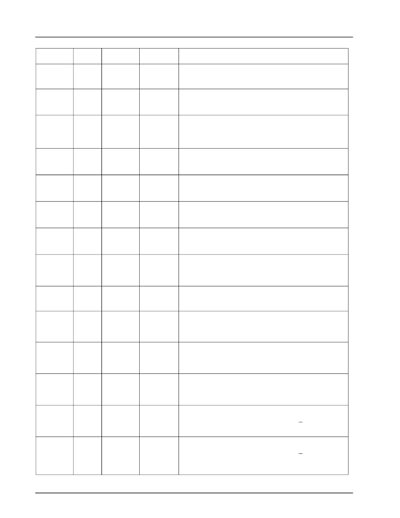
Table 1: Pin Description
CH7009A
4
201-0000-035 Rev 1.1, 5/8/2000
64-Pin
LQFP
14
# Pins
Type
Symbol
Description
1
In/Out
SD
Serial Data Input / Output
This pin functions as the serial data pin of the IIC interface
port, and uses the DVDD supply.
Serial Clock Input
This pin functions as the clock pin of the IIC interface port,
and uses the DVDD supply.
TMDS
TM
Link Swing Control
This pin sets the swing level of the DVI outputs. A 2.4K ohm
resistor should be connected between this pin and TGND using
short and wide traces.
TMDS
TM
Data Channel 0 Outputs
These pins provide the DVI differential outputs for data
channel 0 (blue).
TMDS
TM
Data Channel 1 Outputs
These pins provide the DVI differential outputs for data
channel 1 (green).
TMDS
TM
Data Channel 2 Outputs
These pins provide the DVI differential outputs for data
channel 2 (red).
TMDS
TM
Link Clock Outputs
These pins provide the differential clock output for the DVI
interface corresponding to data on the TDC[0:2] outputs.
Current Set Resistor Input
This pin sets the DAC current. A 140 ohm resistor should be
connected between this pin and GND (DAC ground) using
short and wide traces.
Composite Video
This pin outputs a composite video signal capable of driving a
75 ohm doubly terminated load.
Luma / Green Output
This pin outputs a selectable video signal. The output is
designed to drive a 75 ohm doubly terminated load. The
output can be selected to be s-video luminance or green
.
Chroma / Red Output
This pin outputs a selectable video signal. The output is
designed to drive a 75 ohm doubly terminated load. The
output can be selected to be s-video chrominance or red.
Composite Video / Blue Output
This pin outputs a selectable video signal. The output is
designed to drive a 75 ohm doubly terminated load. The
output can be selected to be composite video or blue.
Crystal Input / External Reference Input
A parallel resonance 14.31818MHz crystal (+ 20 ppm) should
be attached between this pin and XO. However, an external
clock can drive the XI/FIN input.
Crystal Output
A parallel resonance 14.31818MHz crystal (+ 20 ppm) should
be attached between this pin and XI / FIN. However, if an
external CMOS clock is attached to XI/FIN, XO should be left
open.
15
1
In
SC
19
1
In
VSWING
22, 21
2
Out
TDC0,
TDC0*
25, 24
2
Out
TDC1,
TDC1*
28, 27
2
Out
TDC2,
TDC2*
30, 31
2
Out
TLC,
TLC*
35
1
In
ISET
36
1
Out
CVBS
37
1
Out
Y/G
38
1
Out
C/R
39
1
Out
CVBS/B
42
1
In
XI / FIN
43
1
In
XO
相關(guān)PDF資料 |
PDF描述 |
|---|---|
| CH7009A-T | Chrontel CH7009 DVI / TV Output Device |
| CH7303 | Chrontel CH7303 HDTV / DVI Encoder |
| CH8398A | TRUE-COLOR CHRONDAC WITH 16-BIT INTERFACE |
| CHF1206CNT | 20 W Power RF Chip Termination |
| CHF1206CNT500LY | 20 W Power RF Chip Termination |
相關(guān)代理商/技術(shù)參數(shù) |
參數(shù)描述 |
|---|---|
| CH7009A-T | 制造商:未知廠家 制造商全稱:未知廠家 功能描述:Chrontel CH7009 DVI / TV Output Device |
| CH7011A-T | 制造商:未知廠家 制造商全稱:未知廠家 功能描述:Consumer IC |
| CH7012 | 制造商:未知廠家 制造商全稱:未知廠家 功能描述:Chrontel CH7012 TV Output Device |
| CH7012A | 制造商:未知廠家 制造商全稱:未知廠家 功能描述:Chrontel CH7012 TV Output Device |
| CH7012A-T | 制造商:未知廠家 制造商全稱:未知廠家 功能描述:Chrontel CH7012 TV Output Device |
發(fā)布緊急采購,3分鐘左右您將得到回復(fù)。