- 您現(xiàn)在的位置:買賣IC網(wǎng) > PDF目錄298947 > CDQ0303-QS-000T 500 MHz - 6000 MHz RF/MICROWAVE WIDE BAND LOW POWER AMPLIFIER PDF資料下載
參數(shù)資料
| 型號: | CDQ0303-QS-000T |
| 元件分類: | 放大器 |
| 英文描述: | 500 MHz - 6000 MHz RF/MICROWAVE WIDE BAND LOW POWER AMPLIFIER |
| 封裝: | 4 X 4 MM, ULTRA COMPACT, PLASTIC, QS, QFN-16 |
| 文件頁數(shù): | 7/19頁 |
| 文件大小: | 964K |
| 代理商: | CDQ0303-QS-000T |
3236 Scott Boulevard, Santa Clara, California 95054
Phone: (408) 986-5060
Fax: (408) 986-5095
CDQ0303-QS
Advanced Product Information - May 2005
V1.0 (14 of 18)
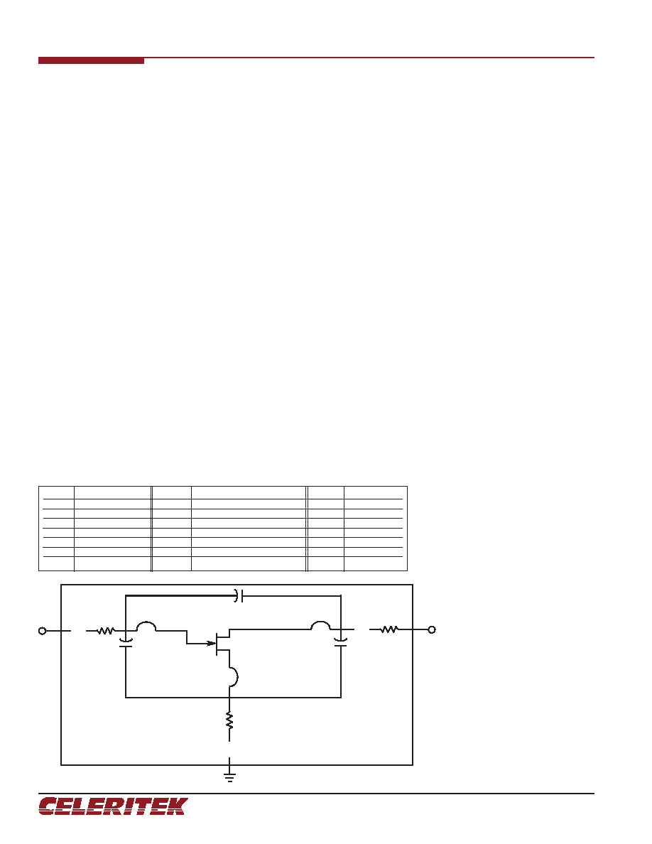
Considerations When Designing for Optimum
Noise Figure Using Noise Parameters
For any two-port network, the noise figure gives a
measure of the amount of noise added to a signal transmitted
through that network. In this data sheet we have given the
NFmin and the corresponding optimum source resistance val-
ues for the device under various bias conditions. NFmin repre-
sents the true minimum noise figure when the device is pre-
sented with an impedance matching network that transforms
the source impedance typically 50 ohms to that optimum noise
matching impedance referred to as Gopt. All stability consid-
erations still apply, of course. If the calculated Rollet stability
factor (K) is less than 1, then the source and load reflection
coefficients must be carefully chosen. For an accurate graphi-
cal depiction of the unstable regions, it is best to draw stability
circles.
In practice the impedance that minimizes the noise
figure is different from the impedance that minimizes the
return loss. Matching techniques such as inductive feedback
will be used to bring the noise match closer to this gain match.
An additional inherent danger of this technique is the
increased instability of the design at higher frequencies. As the
frequency increases the source inductance will also increase,
this increases the amount of feedback to the devices source up
to an oscillation level. This issue can be reduced by carefully
choosing the input and output matching topology so that the
transducer gain is limited at the frequency of potential oscilla-
tion. Design of a high pass / low pass matching network on the
input and output is one solution that addresses this problem.
Careful simulation is essential using the wideband s-parame-
ters provided and can only be achieved through careful model-
ing of all components utilized in the design, including:
1. Accurate high frequency models for all surface
mount components used.
2. Accurate models of the board characteristics
including loss tangents and metal thickness.
3. Use of Via holes and via pads instead of perfect
grounds where used.
In any case if the reflection coefficient of the chosen
matching network is other than Gopt, then the noise figure of
the device will be greater than NFmin. The losses of the
matching circuits are also non-zero and it must be considered
that the noise figure of the completed amplifier is equal to the
noise figure of the device plus the losses of the matching net-
work preceding the device.
The losses of the matching networks are related to the
Q of the components and associated printed circuit board loss.
In general larger gate width devices will typically have a
lower Gopt as compared to smaller gate width devices.
Matching to higher impedance devices requires very hi-Q
components in order to minimize circuit losses. The main rea-
son for using smaller gate width devices is the trade-off of cur-
rent consumption and optimum noise performance. The
CDQ0303-QS is a 600um gate width device has a minimum
noise figure of 0.08 dB and a Gopt of Mag 0.83, Ang 36.63,
making it significantly easier to match than competitive
devices. Associated gain Ga is 20.82 dB.
Device Non-Linear Model
Celeritek develops its own non-linear model based on
its own internal device characterization. The model is verified
in different simulators and compared to the original data from
which it was extracted.
Die Model - Gate Width = 600 m, Optimized for 0.1 GHz to 26.0 GHz
Cgs
1.04 pF
Rg
0.29
Cpd
0.08 pF
Cdg
0.07 pF
Ls
0.04 nH
PCG
0.195 pF
Cds
0.1 pF
Ld
0.1 nH
PCD
0.21 pF
Gm
303 mS
Lg
0.05 nH
PLS
0.085 nH
Ri
2.2 Ohm
BG
5 mil Gold wire (1 mil dia)
PLG
0.525 nH
Tau
0.06 ps
BD
5 mil Gold wire (1 mil dia)
PLD
0.55 nH
Rs
1.28
BS
3 mil Gold wire (1 mil dia)
PCDG
0.005 pF
Rd
1.35
Cpg
0.10 pF
SRL
PLG1
uuuu
C
PCG
C
PCDG
C
PCD
SRL
PLD
WIRE
BD
WIRE
BG
uuuu
WIRE
BS
SRL
PLS
PSFET
Parker Skellern
W=600
The PSFET is a Celeritek imple-
mentation of the Parker Skellern
large signal model. The model is
available as an ADS project file
on-line at: www.celeritek.com
相關(guān)PDF資料 |
PDF描述 |
|---|---|
| CDR105B-100 | Surface Mount Power Inductors |
| CDR105B-101 | Surface Mount Power Inductors |
| CDR105B-120 | Surface Mount Power Inductors |
| CDR105B-121 | Surface Mount Power Inductors |
| CDR105B-150 | Surface Mount Power Inductors |
相關(guān)代理商/技術(shù)參數(shù) |
參數(shù)描述 |
|---|---|
| CDQ0303-QS-0G00 | 制造商:MIMIX 制造商全稱:MIMIX 功能描述:500-6000 MHz Dual, Ultra Low Noise, High IP3 Amplifier |
| CDQ0303-QS-0G0T | 制造商:MIMIX 制造商全稱:MIMIX 功能描述:500-6000 MHz Dual, Ultra Low Noise, High IP3 Amplifier |
| CDQ10473 | 制造商:Texas Instruments 功能描述: |
| CDQ2A12-15D | 制造商:SMC Corporation of America 功能描述:Cylinder |
| CDQ2A20-35D | 制造商:SMC Corporation of America 功能描述:CYLINDER, COMPACT |
發(fā)布緊急采購,3分鐘左右您將得到回復。