- 您現(xiàn)在的位置:買賣IC網 > PDF目錄382861 > AX88140A (Electronic Theatre Controls, Inc.) Fast Ethernet MAC Controller PDF資料下載
參數(shù)資料
| 型號: | AX88140A |
| 廠商: | Electronic Theatre Controls, Inc. |
| 英文描述: | Fast Ethernet MAC Controller |
| 中文描述: | 快速以太網MAC控制器 |
| 文件頁數(shù): | 14/46頁 |
| 文件大小: | 467K |
| 代理商: | AX88140A |
第1頁第2頁第3頁第4頁第5頁第6頁第7頁第8頁第9頁第10頁第11頁第12頁第13頁當前第14頁第15頁第16頁第17頁第18頁第19頁第20頁第21頁第22頁第23頁第24頁第25頁第26頁第27頁第28頁第29頁第30頁第31頁第32頁第33頁第34頁第35頁第36頁第37頁第38頁第39頁第40頁第41頁第42頁第43頁第44頁第45頁第46頁
AX88140A
PRELIMINARY
ASIX ELECTRONICS CORPORATION
14
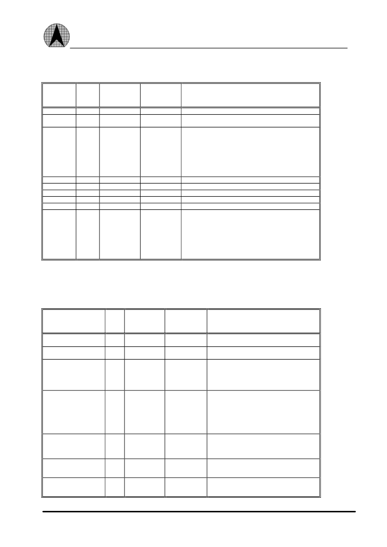
2.3 Boot ROM , Serial ROM , General-purpose signals group
SIGNAL
TYPE
PIN
NUMBER
FOR 160 PIN
112
113
PIN
NUMBER
FOR 144 PIN
102
103
DESCRIPTION
BR_A<0>
BR_A<1>
0
0
Boot ROM address line bit 0.
Boot ROM address line bit 1. This pin also latches the boot ROM
address and control lines by the two external latches.
Boot ROM address and data multiplexed lines bits 7 through 0. In
the first of two consecutive address cycles, these lines contain the
boot ROM address bits 9 through 2; followed by boot ROM
address bits 17 through 10 in the second cycle. During the data
cycle, bits 7 through 0 contain data.
BR_AD<7>
BR_AD<6>
BR_AD<5>
BR_AD<4>
BR_AD<3>
BR_AD<2>
BR_AD<1>
BR_AD<0>
BR_CE#
SR_CK
SR_CS
SR_DI
SR_DO
GENP<7>
GENP<6>
GENP<5>
GENP<4>
GENP<3>
GENP<2>
GENP<1>
GENP<0>
I/O
110,
109,
106,
105,
104,
103,
102,
101
111
88
89
87
86
99,
98,
97,
96,
93,
92,
91,
90
100,
99,
96,
95,
94,
93,
92,
91
101
78
79
77
76
89,
88,
87,
86,
83,
82,
81,
80
O
O
O
O
I
I/O
Boot ROM chip enable.
Serial ROM clock signal.
Serial ROM chip-select signal.
Serial ROM data-in signal.
Serial ROM data-out signal.
General-purpose pins can be used by software as either status pins
or control pins. These pins can be configured by software to
perform either input or output functions.
Tab - 2 Boot ROM , Serial ROM , General-purpose signals group
2.4 MII/SYM/SRL interface signals group
SIGNAL
TYPE PIN
NUMBER
FOR 160 PIN
126
PIN
NUMBER
FOR 144 PIN
112
DESCRIPTION
MCOL
I
Collision detected is asserted when detected by an
external physical layer protocol(PHY) device.
Carrier sense is asserted by the PHY when the media
is active.
Data valid is asserted by an external PHY when
receive data is present on the MRXD/SYRXD lines
and is deasserted at the end of the packet. This signal
should be synchronized with the
MRCLK/SYMRCLK signal.
Receive error asserts when a data decoding error is
detected by an external PHY device. This signal is
synchronized to MRCLK/SYMRCLK and can be
asserted for a minimum of one receive clock. When
asserted during a packet reception, it sets the cyclic
redundancy check(CRC) error bit in the receive
descriptor (RDESO).
MII management data clock is sourced by the
AX88140A to the PHY devices as a timing reference
for the transfer of information on the MII_MDIO
signal.
MII management data input/output transfers control
information and status between the PHY and the
AX88140A.
Indicates the selected port: SRL or MII/SYM. When
asserted, the MII/SYM port is active. When
deasserted, the SRL port is active.
MCRS
I
127
113
MRXDV
I
125
111
MRXERR
I
124
110
MDC
O
116
106
MDIO
I/O
115
105
MII/SRL
O
147
133
相關PDF資料 |
PDF描述 |
|---|---|
| AX88140AP | Fast Ethernet MAC Controller |
| AX88140AQ | Fast Ethernet MAC Controller |
| AX88196 | 10/100BASE 3-in-1 Local CPU Bus Fast Ethernet Controller with Embedded SRAM |
| AX88196L | 10/100BASE 3-in-1 Local CPU Bus Fast Ethernet Controller with Embedded SRAM |
| AX88796 | 3-in-1 Local Bus Fast Ethernet Controller |
相關代理商/技術參數(shù) |
參數(shù)描述 |
|---|---|
| AX88140AP | 制造商:ASIX 制造商全稱:ASIX 功能描述:Fast Ethernet MAC Controller |
| AX88140AQ | 制造商:ASIX 制造商全稱:ASIX 功能描述:Fast Ethernet MAC Controller |
| AX88141 | 制造商:ASIX 制造商全稱:ASIX 功能描述:100BASE-TX/FX PCI BUS FAST ETHERNET MAC CONTROLLER WITH POWER MANAGEMENT |
| AX88170L | 制造商:ASIX 制造商全稱:ASIX 功能描述:USB to Fast Ethernet/HomePNA Controller |
| AX88172 | 制造商:ASI 制造商全稱:ASI 功能描述:USB2.0 TO ETHERNET Device setup guide |
發(fā)布緊急采購,3分鐘左右您將得到回復。