- 您現(xiàn)在的位置:買賣IC網 > PDF目錄358668 > ATF1500 (Atmel Corp.) 44-pin Complex PLD(44腳復雜可編程邏輯器件) PDF資料下載
參數資料
| 型號: | ATF1500 |
| 廠商: | Atmel Corp. |
| 英文描述: | 44-pin Complex PLD(44腳復雜可編程邏輯器件) |
| 中文描述: | 44引腳復雜可編程邏輯器件(44腳復雜可編程邏輯器件) |
| 文件頁數: | 3/10頁 |
| 文件大小: | 195K |
| 代理商: | ATF1500 |

Flash PLD
3
ATF1500 Key Features
Some of the ATF1500 key functional features are summa-
rized below:
Global Bus connected to every macrocell to eliminate
routing bottlenecks, to increase logic utilization and
enable design changes with fixed pin placements.
Independent configurable D- or T-type flip-flop, or
transparent Latch.
Global pin or product term controlled Output Enable for
each I/O.
Global pin or product term controlled Clock or Reset for
each flip-flop in the macrocell.
Macrocell configuration providing a Combinatorial output
along with a buried register feedback.
Pin-controlled or automatic power-down options to
reduce overall system power consumption.
Slew rate control for each output to reduce overall
system noise.
Programming time of less than 10 seconds.
ATF1500 Bus-friendly Pin-keeper
Inputs and I/Os
All Input and I/O pins on the ATF1500 have bus-friendly
“
data-keeper
”
circuits. When any pin is driven high or low
and then subsequently left floating, it will stay at that previ-
ous high or low level. This prevents the inputs or I/Os from
floating to an intermediate voltage, and hence reduces
power consumption, system noise and eliminating the need
for external pull-up resistors.
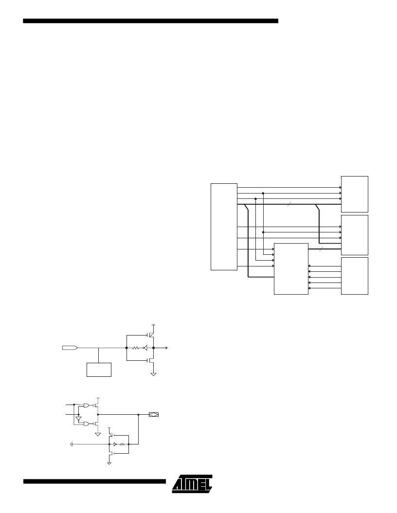
Figure 3.
ATF1500 Input and I/O Circuitry
ATF1500 Design Example – Memory
and I/O Interface to a Single-chip
Microprocessor
This is a microprocessor based design to display large vol-
umes of text on a 2 line by 16 character LCD display using
a simple keypad. The design was implemented using a sin-
gle microprocessor chip that interfaced to the LCD display,
a 5-key keypad, a 4 MB Flash memory and an ATF1500
CPLD (see Figure 4). The Flash memory stores the text.
Since the single microprocessor chip does not have an
external address or data bus, these signals must be gener-
ated by the ATF1500 device via control signals from the I/O
ports on the CPU.
Figure 4.
System Block Diagram
The customer implemented the design using the Data I/O
Synario Development tool. Figure 5 shows the block dia-
gram of the interface design for the logic in the ATF1500.
The design consists of three logic blocks: Address Counter
(ADDRCNTR); Data Multiplexer (DATAMUX) and Switch
Latch (SWLATCH) blocks. Since all the data in the Flash
memory is in the form of text strings, the address of the first
character of a string can be loaded into the 19-bit counter.
The counter is then clocked each time a byte is read by the
CPU, making the next character available immediately. The
SWLATCH block contains latches to hold the keypad data.
The DATAMUX block enables the CPU to read not just the
keypad data, but also the condition of the counter.
100K
V
CC
PCIRCUIT
INPUT
100K
V
CC
DATA
OE
I/O
V
CC
E
R_W
RS0
RS1
A[18:0]
Enter
Up
Down
Right
Left
Data[7:0]
PB3
PB2
PB0
PA[7:0]
Single
Chip
Micro
PB5
PB6
PB4
PB1
LCD Display
E
R/W
RS0
D[7:0]
4 Mbit Flash
CS
R/W
OE
D[7:0]
A[18:0]
Keypad
Key0
Key1
Key2
Key3
Key4
ATF1500
19
8
相關PDF資料 |
PDF描述 |
|---|---|
| ATF1516ASL | High-performance EE-based CPLD(高性能可電擦除復雜可編程邏輯器件(CPLD)) |
| ATtiny12L | 8-Bit AVR Microcontroller with 1K bytes Flash(8位AVR技術微控制器(帶1K字節(jié)閃速存儲器 )) |
| AXH010A0MZ | 1-OUTPUT 15 W DC-DC REG PWR SUPPLY MODULE |
| BA545AL | Low-leakage diode |
| BAP55L | Silicon PIN diode |
相關代理商/技術參數 |
參數描述 |
|---|---|
| ATF1500-7AC | 制造商:Atmel Corporation 功能描述: |
| ATF1500A | 制造商:ATMEL 制造商全稱:ATMEL Corporation 功能描述:Highperformance EPLD |
| ATF1500A(L) | 制造商:未知廠家 制造商全稱:未知廠家 功能描述:ATF1500A(L) [Updated 6/99. 17 Pages] 1500 gate electrically erasable CPLD. 44 pins |
| ATF1500A_05 | 制造商:ATMEL 制造商全稱:ATMEL Corporation 功能描述:Highperformance EPLD |
| ATF1500A-10AC | 功能描述:CPLD - 復雜可編程邏輯器件 CPLD 32 MACROCELL CMPTBLE w/F1500 RoHS:否 制造商:Lattice 系列: 存儲類型:EEPROM 大電池數量:128 最大工作頻率:333 MHz 延遲時間:2.7 ns 可編程輸入/輸出端數量:64 工作電源電壓:3.3 V 最大工作溫度:+ 90 C 最小工作溫度:0 C 封裝 / 箱體:TQFP-100 |
發(fā)布緊急采購,3分鐘左右您將得到回復。