- 您現(xiàn)在的位置:買賣IC網(wǎng) > PDF目錄381452 > AT45DB011D-MU (ATMEL CORP) 1-megabit 2.7-volt DataFlash PDF資料下載
參數(shù)資料
| 型號(hào): | AT45DB011D-MU |
| 廠商: | ATMEL CORP |
| 元件分類: | DRAM |
| 英文描述: | 1-megabit 2.7-volt DataFlash |
| 中文描述: | 1M X 1 FLASH 2.7V PROM, DSO8 |
| 封裝: | 6 X 5 MM, 1 MM HEIGHT, GREEN, MLF-8 |
| 文件頁(yè)數(shù): | 17/52頁(yè) |
| 文件大?。?/td> | 1107K |
| 代理商: | AT45DB011D-MU |
第1頁(yè)第2頁(yè)第3頁(yè)第4頁(yè)第5頁(yè)第6頁(yè)第7頁(yè)第8頁(yè)第9頁(yè)第10頁(yè)第11頁(yè)第12頁(yè)第13頁(yè)第14頁(yè)第15頁(yè)第16頁(yè)當(dāng)前第17頁(yè)第18頁(yè)第19頁(yè)第20頁(yè)第21頁(yè)第22頁(yè)第23頁(yè)第24頁(yè)第25頁(yè)第26頁(yè)第27頁(yè)第28頁(yè)第29頁(yè)第30頁(yè)第31頁(yè)第32頁(yè)第33頁(yè)第34頁(yè)第35頁(yè)第36頁(yè)第37頁(yè)第38頁(yè)第39頁(yè)第40頁(yè)第41頁(yè)第42頁(yè)第43頁(yè)第44頁(yè)第45頁(yè)第46頁(yè)第47頁(yè)第48頁(yè)第49頁(yè)第50頁(yè)第51頁(yè)第52頁(yè)
17
3639B–DFLASH–02/07
AT45DB011D [Preliminary]
9.1.3
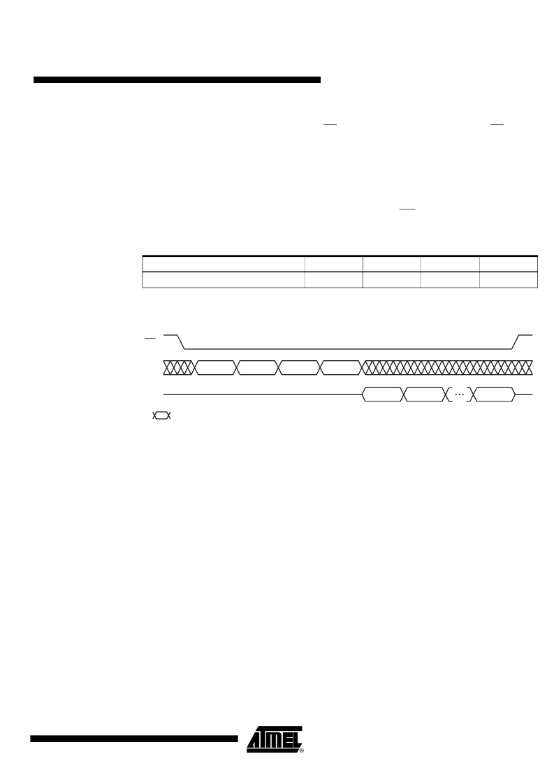
Read Sector Protection Register Command
To read the Sector Protection Register, the CS pin must first be asserted. Once the CS pin has
been asserted, an opcode of 32H and 3 dummy bytes must be clocked in via the SI pin. After the
last bit of the opcode and dummy bytes have been clocked in, any additional clock pulses on the
SCK pins will result in data for the content of the Sector Protection Register being output on the
SO pin. The first byte corresponds to sector 0 (0a, 0b), the second byte corresponds to sector 1,
the third byte corresponds to sector 2, and the last byte (byte 4) corresponds to sector 3. Once
the last byte of the Sector Protection Register has been clocked out, any additional clock pulses
will result in undefined data being output on the SO pin. The CS must be deasserted to termi-
nate the Read Sector Protection Register operation and put the output into a high-impedance
state.
Note:
xx = Dummy Byte
Figure 9-4.
Read Sector Protection Register
9.1.4
Various Aspects About the Sector Protection Register
The Sector Protection Register is subject to a limit of 10,000 erase/program cycles. Users are
encouraged to carefully evaluate the number of times the Sector Protection Register will be
modified during the course of the applications’ life cycle. If the application requires that the Sec-
tor Protection Register be modified more than the specified limit of 10,000 cycles because the
application needs to temporarily unprotect individual sectors (sector protection remains enabled
while the Sector Protection Register is reprogrammed), then the application will need to limit this
practice. Instead, a combination of temporarily unprotecting individual sectors along with dis-
abling sector protection completely will need to be implemented by the application to ensure that
the limit of 10,000 cycles is not exceeded.
Command
Byte 1
Byte 2
Byte 3
Byte 4
Read Sector Protection Register
32H
xxH
xxH
xxH
Opcode
X
X
X
Data Byte
n
Data Byte
n + 1
CS
Data Byte
n + 3
SI
SO
Each transition
represents
8
b
its
相關(guān)PDF資料 |
PDF描述 |
|---|---|
| AT45DB011D-SSU | 1-megabit 2.7-volt DataFlash |
| AT45DB011D-SU | 1-megabit 2.7-volt DataFlash |
| AT45DB011 | 1-megabit 2.7-volt Only Serial DataFlash(1M位 2.7V串行數(shù)據(jù)閃速存儲(chǔ)器) |
| AT45DB021B-CU | 2-megabit 2.7-volt Only DataFlash |
| AT45DB021B-RU | 2-megabit 2.7-volt Only DataFlash |
相關(guān)代理商/技術(shù)參數(shù) |
參數(shù)描述 |
|---|---|
| AT45DB011D-SH | 制造商:Atmel Corporation 功能描述:DATAFLASH SERIAL 20MHZ 1MB 45DB011 |
| AT45DB011D-SH SL954 | 制造商:Adesto Technologies Corporation 功能描述:IC FLASH 1MBIT 66MHZ 8SOIC |
| AT45DB011D-SH-B | 功能描述:閃存 1M 2.7-3.6V, 66Mhz Serial 閃存 RoHS:否 制造商:ON Semiconductor 數(shù)據(jù)總線寬度:1 bit 存儲(chǔ)類型:Flash 存儲(chǔ)容量:2 MB 結(jié)構(gòu):256 K x 8 定時(shí)類型: 接口類型:SPI 訪問(wèn)時(shí)間: 電源電壓-最大:3.6 V 電源電壓-最小:2.3 V 最大工作電流:15 mA 工作溫度:- 40 C to + 85 C 安裝風(fēng)格:SMD/SMT 封裝 / 箱體: 封裝:Reel |
| AT45DB011D-SHET-T | 制造商:Adesto Technologies Corporation 功能描述:8-SOIC-W, IND TEMP, 2.7V, T&R - Tape and Reel |
| AT45DB011D-SHGK-T | 制造商:Adesto Technologies Corporation 功能描述:8-SOIC-W, IND TEMP, 2.7V, T&R - Tape and Reel |
發(fā)布緊急采購(gòu),3分鐘左右您將得到回復(fù)。