- 您現(xiàn)在的位置:買賣IC網(wǎng) > PDF目錄378405 > AND8112 (ON SEMICONDUCTOR) A Quasi-Resonant SPICE Model Eases Feedback Loop Designs PDF資料下載
參數(shù)資料
| 型號: | AND8112 |
| 廠商: | ON SEMICONDUCTOR |
| 英文描述: | A Quasi-Resonant SPICE Model Eases Feedback Loop Designs |
| 中文描述: | 阿準(zhǔn)諧振SPICE模型反饋環(huán)的設(shè)計更易 |
| 文件頁數(shù): | 7/12頁 |
| 文件大?。?/td> | 205K |
| 代理商: | AND8112 |
AND8112/D
http://onsemi.com
7
The following table summarizes the main equations upon which our model is based:
Delay between the power switch opening and the start of the ener-
gy transfer to secondary side:
t1
LP
Ctot
Vg
Vg
V
N
ton
Delay between the core reset completion and the next turn on of
the power switch (Note 1):
t2
LP
Ctot
Equivalent input resistance:
Re(ton)
2
LP
ton
2
t1
t2
[(N
Vg)
V]
ton
V
Switching Frequency:
fSW
1
t1
t2
(N
Vg)
V
ton
V
Average input current:
I1(t)
VgRe(ton)
Average output current:
I2(t)
Vg
V
I1(t)
eff
NOTE:
: even if the proposed value appears to us as the
optimal one, SMPS designers might make a
different choice for
t2
. That is why, if the model
proposes
t2
LP
value, you can modify this simulation parameter
to stick to your application in case valley
switching is not considered.
Ctot
as default
Implementing the SPICE Model with the
LossFree Network
As exemplified by Figure 6, the model shall emulate an
input resistor being
t
on
dependent and then transmit a power
following equation 23. Different ways exist to implement
this topology in Spice. INTUSOFT’s IsSpice authorizes
behavioral resistors, e.g. following any particular ohmic
evolution with time, voltage, current etc. For instance, the
following code would be accepted by the simulator:
R1 1 2 R = 2.0 * v(1)^0.5 + 3.0*v(2)*time + v(2)*sqrt(temp)
Unfortunately, despite its obvious interest, this code is not
very portable and would constrain the model usage to
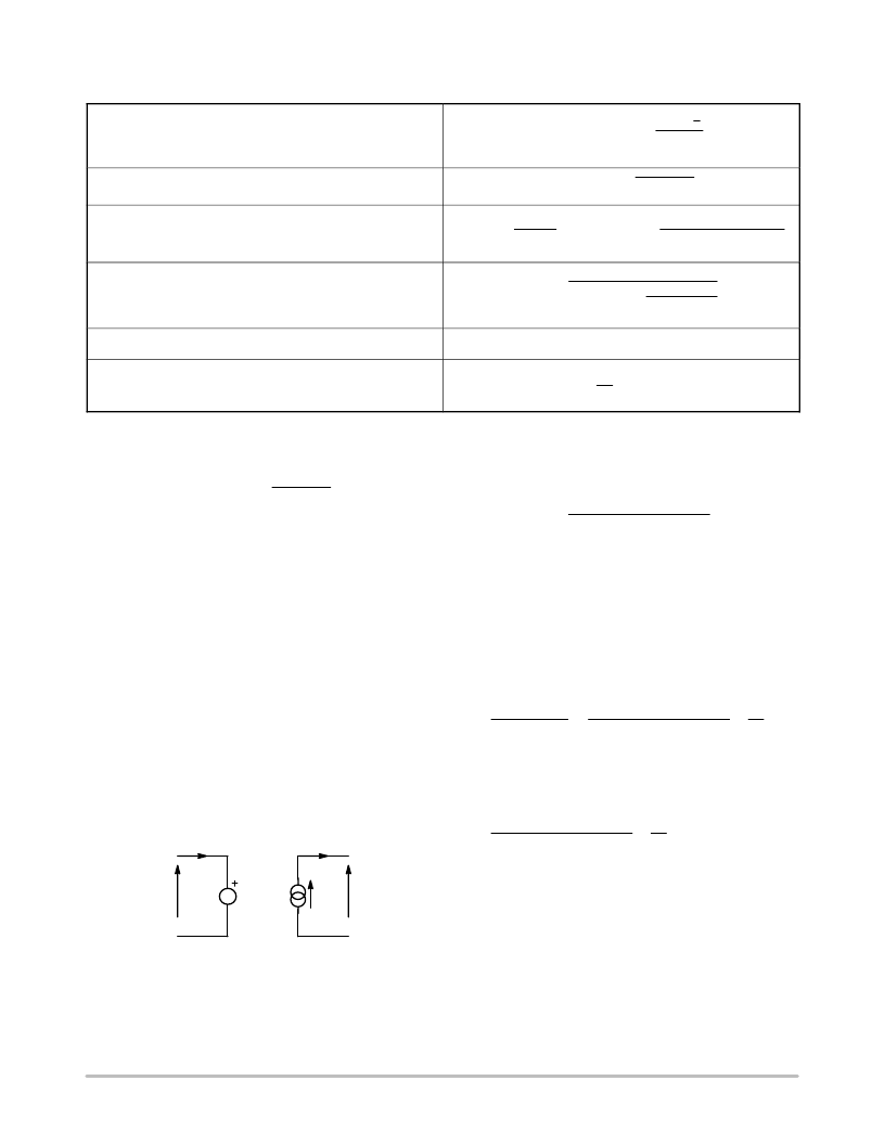
IsSpice only. Figure 9 offers a more practical association
using behavioral voltage and current sources [2]:
Et
Gd
Figure 9. Implementing the DCM Model via Two
Controlled Elements
I
2
I
1
V
1
V
2
The input voltage source being supposed to emulate a
resistance, its expression shall be in the form of:
Et = I
1
x Re where Re is simply equation 22, thus:
2
LP
(V
ton
Et
I1
N
Vg)
V
(eq. 41)
where
t
on
is an input port of the model, imposed by the
control loop. In the final model, this value will be derived
from L
P
and the peak current given by the error voltage
divided by R
sense
, where V, V
g
and N are to be passed or
sensed by the model.
The output current source together with V
2
shall deliver
the output power as imposed by equation 22. Thus, i
2
generation shall follow:
I2
Rin(eq)
i1
2
v2
2
LP
(V
N
Vg)
ton
V
i1
2
v2
(eq. 42)
Also, one can introduce the efficiency by simply
multiplying the I
2
current source by {eff}, where
eff
is a
parameter entered by the user in the model. Hence, I
2
can be
written as:
2
LP
(V
N
Vg)
ton
V
I2
i1
2
v2
eff
(eq. 43)
相關(guān)PDF資料 |
PDF描述 |
|---|---|
| AND8116 | Integrated Relay/Inductive Load Drivers for Industrial and Automotive Applications |
| AND8116D | Integrated Relay/Inductive Load Drivers for Industrial and Automotive Applications |
| AND8130 | Analog Switch Allows USB Switching at Low Voltages |
| AND8139 | Ultra-Low Voltage MiniGate Devices Solve 1.2 V Interface Problems |
| AND8139D | Ultra-Low Voltage MiniGate Devices Solve 1.2 V Interface Problems |
相關(guān)代理商/技術(shù)參數(shù) |
參數(shù)描述 |
|---|---|
| AND8116 | 制造商:ONSEMI 制造商全稱:ON Semiconductor 功能描述:Integrated Relay/Inductive Load Drivers for Industrial and Automotive Applications |
| AND8116D | 制造商:ONSEMI 制造商全稱:ON Semiconductor 功能描述:Integrated Relay/Inductive Load Drivers for Industrial and Automotive Applications |
| AND8130 | 制造商:ONSEMI 制造商全稱:ON Semiconductor 功能描述:Analog Switch Allows USB Switching at Low Voltages |
| AND8130/D | 制造商:ONSEMI 制造商全稱:ON Semiconductor 功能描述:Analog Switch Allows USB Switching at Low Voltages |
| AND8139 | 制造商:ONSEMI 制造商全稱:ON Semiconductor 功能描述:Ultra-Low Voltage MiniGate Devices Solve 1.2 V Interface Problems |
發(fā)布緊急采購,3分鐘左右您將得到回復(fù)。