- 您現(xiàn)在的位置:買賣IC網(wǎng) > PDF目錄375330 > AND8020D (Analog Devices, Inc.) Termination of ECL Logic Devices with EF (Emitter Follower) OUTPUT Structure PDF資料下載
參數(shù)資料
| 型號: | AND8020D |
| 廠商: | Analog Devices, Inc. |
| 英文描述: | Termination of ECL Logic Devices with EF (Emitter Follower) OUTPUT Structure |
| 中文描述: | ECL邏輯器件的終止與英法(發(fā)射極跟隨器)輸出結(jié)構(gòu) |
| 文件頁數(shù): | 13/18頁 |
| 文件大小: | 168K |
| 代理商: | AND8020D |
AND8020/D
http://onsemi.com
13
For the 10E series (ECL mode operation),
where: V
OH
= 0.9 V, V
SWING
= 0.85 V, V
EE
= 5.2 V:
(
0.9)
Rt
(
5.2)
Z0
Rs
0.531
Z0
* Z0
Rs
Rt
7.10
(eq. 38)
For the 100E series (ECL mode operation),
where: V
OH
= 0.955 V, V
SWING
= 0.75 V, V
EE
= 4.5 V:
(
0.955)
Rt
(
4.5)
Rs
Z0
0.468
Z0
* Z0
Rs
Rt
6.57
(eq. 39)
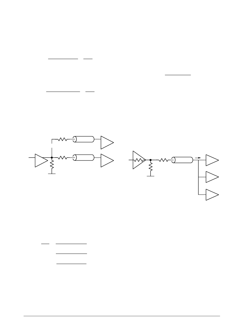
Parallel Fanout of Series Termination
An extension of the series termination technique, using
parallel fanout, eliminates the problem of lumped loading at
the expense of extra transmission lines (Figure 17).
*TLine Z
0
R
Sn
Receiver n
Figure 17. Parallel Fanout Using Series Termination
*TLine Z
0
R
S
1
Receiver 1
Driver
R
t
V
EE
Nnumber of lines
Figure 17 shows a modification of the series termination
scheme in which several series terminated lines in parallel
fanout are driven using a single ECL gate. The principle
concern when applying this technique is to maintain the
current in the output emitter follower below the maximum
rated value. The value for R
t
can be calculated by viewing
the circuit in terms of conductances.
Goutput
G1
G2
G
n
(eq. 40)
From Table B, for each of the series:
1
( Rt)
1
(
* Z01
RS1)
KZ
0
1
(
* Z02
RS2)
KZ
0
1
(
* Z0
RS)
n
KZ
0
(eq. 41)
Where:
n
= Number of Parallel Circuits
When:
Z01
Then R
t
is calculated as:
Z02
Z0 , and RS1
RS2
RS
n
(eq. 42)
Rt
(KZ0* Z0
Rs)
r
n
(eq. 43)
When a single series terminated line is driving more than
a single receiver, the maximum number of loads must be
addressed. The factor limiting the number of loads is the DC
voltage drop across the series termination resistor caused by
the summary input currents I
T
during the receivers quiescent
high state. Noise margin loss, NM
loss
, will probably
determine the acceptable DC voltage drop limit across R
s
.
NMloss
IT* ( Rs
Where:
I
T
= Sum of IINH Currents
R
O
= Output Impedance of the Driver Gate
R
S
= Termination Resistance
RO)
(eq. 44)
Figure 18. Noise Margin Loss Example
*TLine Z
0
R
S
Receiver 1
Driver
R
t
V
EE
R
O
Receiver 2
Receiver N
I
T
For the majority of ECL devices typical maximum value
for quiescent high state input current is 150 uA. Thus, for the
circuit shown in Figure 18, in which three gate loads are
present in a 50
environment, the loss in high state noise
margin is calculated as:
NMloss
3 *
150 mA * 50
This represents a potential shift in the V
OH
level of
22.5 mV.
22.5 mV
(eq. 45)
相關(guān)PDF資料 |
PDF描述 |
|---|---|
| ANP-C-115 | JT 79C 79#22D PIN RECP |
| ANPC-185 | GPS Antenna for Automotive Aftermarket Applications |
| AO3400 | N-Channel Enhancement Mode Field Effect Transistor |
| AO3400L | N-Channel Enhancement Mode Field Effect Transistor |
| AO3401A | P-Channel Enhancement Mode Field Effect Transistor |
相關(guān)代理商/技術(shù)參數(shù) |
參數(shù)描述 |
|---|---|
| AND8028 | 制造商:ONSEMI 制造商全稱:ON Semiconductor 功能描述:Precision Sub-One Volt 1.7 Ampere Output LDO |
| AND8028D | 制造商:ONSEMI 制造商全稱:ON Semiconductor 功能描述:Precision Sub-One Volt 1.7 Ampere Output LDO |
| AND8031 | 制造商:ONSEMI 制造商全稱:ON Semiconductor 功能描述:Isolated Precision Regulation of a Single 1.8 Volt Output from a Universal Line Input |
| AND8031D | 制造商:ONSEMI 制造商全稱:ON Semiconductor 功能描述:Isolated Precision Regulation of a Single 1.8 Volt Output from a Universal Line Input |
| AND8039 | 制造商:ONSEMI 制造商全稱:ON Semiconductor 功能描述:The One-Transistor Forward Converter |
發(fā)布緊急采購,3分鐘左右您將得到回復。