- 您現在的位置:買賣IC網 > PDF目錄373857 > AD14160 (Analog Devices, Inc.) Quad-SHARC DSP Multiprocessor Family PDF資料下載
參數資料
| 型號: | AD14160 |
| 廠商: | Analog Devices, Inc. |
| 英文描述: | Quad-SHARC DSP Multiprocessor Family |
| 中文描述: | 四SHARC處理器DSP的多處理器家族 |
| 文件頁數: | 38/52頁 |
| 文件大小: | 1193K |
| 代理商: | AD14160 |
第1頁第2頁第3頁第4頁第5頁第6頁第7頁第8頁第9頁第10頁第11頁第12頁第13頁第14頁第15頁第16頁第17頁第18頁第19頁第20頁第21頁第22頁第23頁第24頁第25頁第26頁第27頁第28頁第29頁第30頁第31頁第32頁第33頁第34頁第35頁第36頁第37頁當前第38頁第39頁第40頁第41頁第42頁第43頁第44頁第45頁第46頁第47頁第48頁第49頁第50頁第51頁第52頁
AD14160/AD14160L
–38–
REV. A
TEST CONDITIONS
Output Disable Time
Output pins are considered to be disabled when they stop driv-
ing, go into a high impedance state, and start to decay from
their output high or low voltage. The time for the voltage on the
bus to decay by
V is dependent on the capacitive load, C
L
, and
the load current, I
L
. This decay time can be approximated by
the following equation:
t
DECAY
=
C
L
V
I
L
The output disable time, t
DIS
, is the difference between t
MEASURED
and t
DECAY
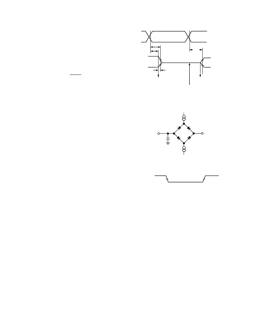
as shown in Figure 28. The time t
MEASURED
is the
interval from when the reference signal switches to when the
output voltage decays
V from the measured output high or
output low voltage. t
DECAY
is calculated with test loads C
L
and
I
L
, and with
V equal to 0.5 V.
Output Enable Time
Output pins are considered to be enabled when they have made
a transition from a high impedance state to when they start
driving. The output enable time, t
ENA
, is the interval from when
a reference signal reaches a high or low voltage level to when the
output has reached a specified high or low trip point, as shown
in the Output Enable/Disable diagram (Figure 28). If multiple
pins (such as the data bus) are enabled, the measurement value
is that of the first pin to start driving.
Example System Hold Time Calculation
To determine the data output hold time in a particular system,
first calculate t
DECAY
using the equation given above. Choose
V to be the difference between the ADSP-2106x’s output
voltage and the input threshold for the device requiring the hold
time. A typical
V will be 0.4 V. C
L
is the total bus capacitance
(per data line), and I
L
is the total leakage or three-state current
(per data line). The hold time will be t
DECAY
plus the minimum
disable time (i.e., t
HDWD
for the write cycle).
REFERENCE
SIGNAL
t
DIS
OUTPUT STARTS
DRIVING
V
OH (MEASURED)
–
D
V
V
OL (MEASURED)
+
D
V
t
DECAY
t
MEASURED
V
OH (MEASURED)
V
OL (MEASURED)
2.0V
1.0V
V
OH (MEASURED)
V
OL (MEASURED)
HIGH-IMPEDANCE STATE.
TEST CONDITIONS CAUSE
THIS VOLTAGE TO BE
APPROXIMATELY 1.5V
OUTPUT STOPS
DRIVING
t
ENA
Figure 28. Output Enable/Disable
+1.5V
50pF
TO
OUTPUT
PIN
I
OL
I
OH
Figure 29. Equivalent Device Loading for AC Measure-
ments (Includes All Fixtures)
INPUT OR
OUTPUT
1.5V
1.5V
Figure 30. Voltage Reference Levels for AC Measurements
(Except Output Enable/Disable)
Capacitive Loading
Output delays and holds are based on standard capacitive loads:
50 pF on all pins (see Figure 29). The delay and hold specifica-
tions given should be derated by a factor of 1.5 ns/50 pF for
loads other than the nominal value of 50 pF. Figures 31, 32, 33
and 34 show how output rise time varies with capacitance.
Figures 35 and 36 graphically show how output delays and
holds vary with load capacitance. (Note that these graphs or
derating does not apply to output disable delays; see the previ-
ous section Output Disable Time under Test Conditions.) The
graphs of Figures 31 through 36 may not be linear outside the
ranges shown.
相關PDF資料 |
PDF描述 |
|---|---|
| AD14160BB-4 | Quad-SHARC DSP Multiprocessor Family |
| AD14160L | Quad-SHARC DSP Multiprocessor Family |
| AD14160LBB-4 | ECONOLINE: RD & RC - Dual Output from a Single Input Rail- 1kVDC & 2kVDC Isolation- Power Sharing on Output- Custom Solutions Available- UL94V-0 Package Material- Efficiency to 86% |
| AD14160LKB-4 | Quad-SHARC DSP Multiprocessor Family |
| AD1555-AD1556 | 24-Bit ADC WITH LOW NOISE PGA |
相關代理商/技術參數 |
參數描述 |
|---|---|
| AD14160BB-4 | 制造商:Rochester Electronics LLC 功能描述:- Bulk |
| AD14160KB-4 | 制造商:Rochester Electronics LLC 功能描述:- Bulk |
| AD14160L | 制造商:AD 制造商全稱:Analog Devices 功能描述:Quad-SHARC DSP Multiprocessor Family |
| AD14160LBB-4 | 制造商:AD 制造商全稱:Analog Devices 功能描述:Quad-SHARC DSP Multiprocessor Family |
| AD14160LKB-4 | 制造商:Rochester Electronics LLC 功能描述:- Bulk |
發(fā)布緊急采購,3分鐘左右您將得到回復。