- 您現(xiàn)在的位置:買賣IC網(wǎng) > PDF目錄122717 > 9LPRS501SKLF (INTEGRATED DEVICE TECHNOLOGY INC) SPECIALTY MICROPROCESSOR CIRCUIT, PQCC64 PDF資料下載
參數(shù)資料
| 型號: | 9LPRS501SKLF |
| 廠商: | INTEGRATED DEVICE TECHNOLOGY INC |
| 元件分類: | 微控制器/微處理器 |
| 英文描述: | SPECIALTY MICROPROCESSOR CIRCUIT, PQCC64 |
| 封裝: | ROHS COMPLIANT, PLASTIC, MLF-64 |
| 文件頁數(shù): | 26/27頁 |
| 文件大小: | 228K |
| 代理商: | 9LPRS501SKLF |
第1頁第2頁第3頁第4頁第5頁第6頁第7頁第8頁第9頁第10頁第11頁第12頁第13頁第14頁第15頁第16頁第17頁第18頁第19頁第20頁第21頁第22頁第23頁第24頁第25頁當前第26頁第27頁
IDTTM/ICSTM
64-pin CK505 w/Fully Integrated Voltage Regulator + Integrated Series Resistor
1121G—05/19/11
Advance Information
ICS9LPRS501
64-PIN CK505 W/FULLY INTEGRATED VOLTAGE REGULATOR + INTEGRATED SERIES RESISTOR
8
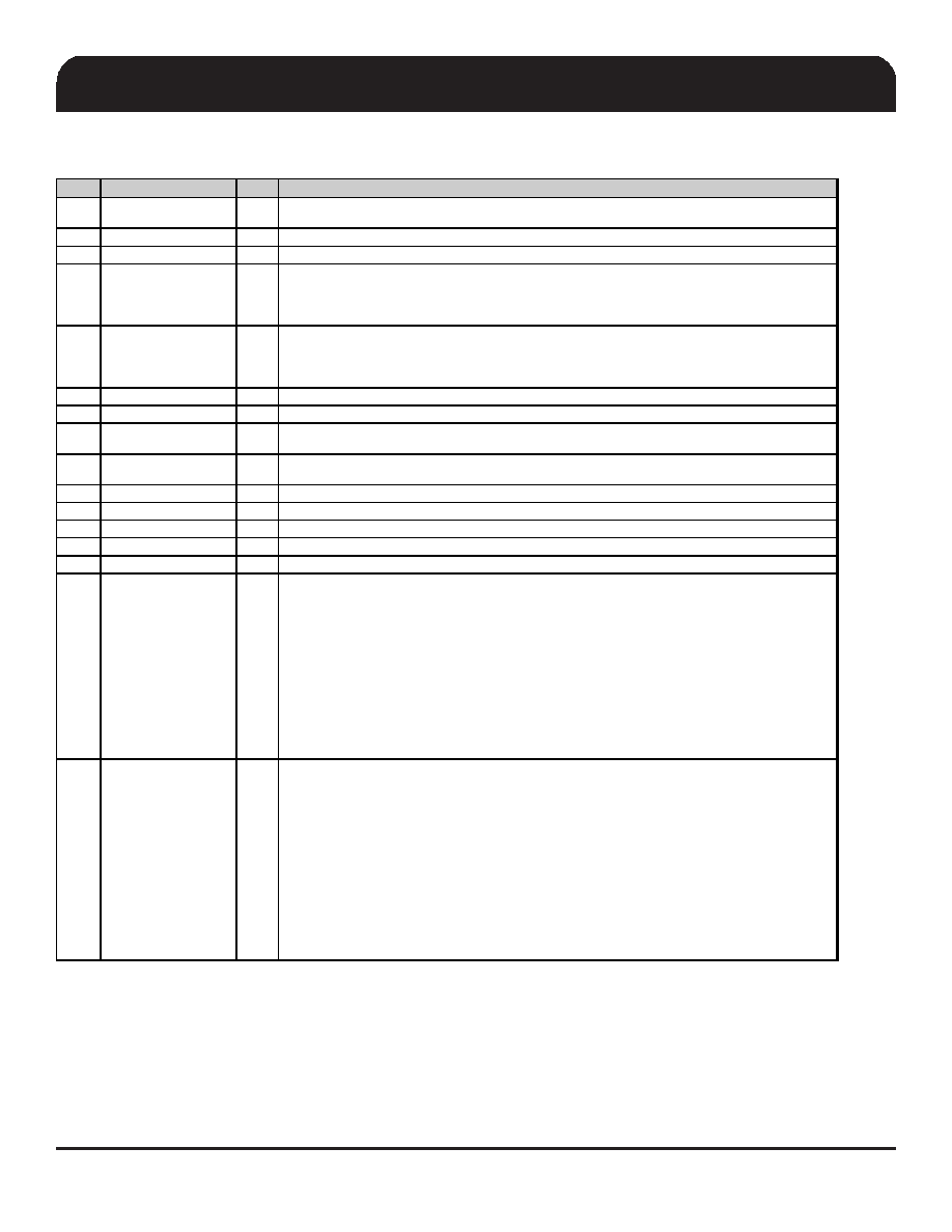
MLF Pin Description (Continued)
PIN #
PIN NAME
TYPE
DESCRIPTION
17
USB_48MHz/FSLA
I/O
Fixed 48MHz USB clock output. 3.3V./ 3.3V tolerant input for CPU frequency selection. Refer to input
electrical characteristics for Vil_FS and Vih_FS values.
18
GND48
PWR Ground pin for the 48MHz outputs.
19
VDD96_IO
PWR Power supply for DOT96 outputs, VDD96_IO is 1.05 to 3.3V with +/-5% tolerance
20
DOTT_96/SRCT0
OUT
True clock of SRC or DOT96. The power-up default function is SRC0. After powerup, this pin function
may be changed to DOT96 via SMBus Byte 1, bit 7 as follows:
0= SRC0
1=DOT96
21
DOTC_96/SRCC0
OUT
Complement clock of SRC or DOT96. The power-up default function is SRC0#. After powerup, this pin
function may be changed to DOT96# via SMBus Byte 1, bit 7 as follows
0= SRC0#
1=DOT96#
22
GND
PWR Ground pin for the DOT96 clocks.
23
VDD
PWR Power supply for SRC / SE1 and SE2 clocks, 3.3V nominal.
24
SRCT1/SE1
OUT
True clock of differential SRC1 clock pair / 3.3V single-ended output. The powerup default is 100 MHz
SRC, -0.5% downspread. The pin function may be changed via SMBus B1b[4:1]
25
SRCC1/SE2
OUT
Complement clock of differential SRC1 clock pair / 3.3V single-ended output. The powerup default is 100
MHz SRC, -0.5% downspread. The pin function may be changed via SMBus B1b[4:1]
26
GND
PWR Ground pin for SRC / SE1 and SE2 clocks, PLL3.
27
VDDPLL3_IO
PWR Power supply for PLL3 output. VDDPLL3_IO is 1.05 to 3.3V with +/-5% tolerance
28
SRCT2/SATAT
OUT
True clock of differential SRC/SATA clock pair.
29
SRCC2/SATAC
OUT
Complement clock of differential SRC/SATA clock pair.
30
GNDSRC
PWR Ground pin for SRC clocks.
31
SRCT3/CR#_C
I/O
True clock of differential SRC clock pair/ Clock Request control C for either SRC0 or SRC2 pair
The power-up default is SRCCLK3 output, but this pin may also be used as a Clock Request control of
SRC pair 0 or SRC pair 2 via SMBus. Before configuring this pin as a Clock Request Pin, the SRC3
output must first be disabled in byte 4, bit 7 of SMBus address space . After the SRC3 output is
disabled, the pin can then be set to serve as a Clock Request pin for either SRC pair 2 or pair 0 using
the CR#_C_EN bit located in byte 5 of SMBUs address space.
Byte 5, bit 3
0 = SRC3 enabled (default)
1= CR#_C enabled. Byte 5, bit 2 controls whether CR#_C controls SRC0 or SRC2 pair
Byte 5, bit 2
0 = CR#_C controls SRC0 pair (default),
1= CR#_C controls SRC2 pair
32
SRCC3/CR#_D
I/O
Complementary clock of differential SRC clock pair/ Clock Request control D for either SRC1 or SRC4
pair
The power-up default is SRCCLK3 output, but this pin may also be used as a Clock Request control of
SRC pair 1 or SRC pair 4 via SMBus. Before configuring this pin as a Clock Request Pin, the SRC3
output must first be disabled in byte 4, bit 7 of SMBus address space . After the SRC3 output is
disabled, the pin can then be set to serve as a Clock Request pin for either SRC pair 1 or pair 4 using
the CR#_D_EN bit located in byte 5 of SMBUs address space.
Byte 5, bit 1
0 = SRC3 enabled (default)
1= CR#_D enabled. Byte 5, bit 0 controls whether CR#_D controls SRC1 or SRC4 pair
Byte 5, bit 0
0 = CR#_D controls SRC1 pair (default),
1= CR#_D controls SRC4 pair
相關PDF資料 |
PDF描述 |
|---|---|
| 9LPRS545CFLFT | SPECIALTY MICROPROCESSOR CIRCUIT, PDSO48 |
| 9173B-01CS08LFT | 75 MHz, VIDEO CLOCK GENERATOR, PDSO8 |
| 951601AFLFT | 66.66 MHz, PROC SPECIFIC CLOCK GENERATOR, PDSO48 |
| 954201BFLFT | 400 MHz, PROC SPECIFIC CLOCK GENERATOR, PDSO56 |
| 935271490512 | 4 CHANNEL(S), 5M bps, SERIAL COMM CONTROLLER, PQCC68 |
相關代理商/技術參數(shù) |
參數(shù)描述 |
|---|---|
| 9LPRS501SKLFT | 功能描述:時鐘合成器/抖動清除器 RoHS:否 制造商:Skyworks Solutions, Inc. 輸出端數(shù)量: 輸出電平: 最大輸出頻率: 輸入電平: 最大輸入頻率:6.1 GHz 電源電壓-最大:3.3 V 電源電壓-最小:2.7 V 封裝 / 箱體:TSSOP-28 封裝:Reel |
| 9LPRS501YGLFT | 制造商:IDT 制造商全稱:Integrated Device Technology 功能描述:64-PIN CK505 W/FULLY INTEGRATED VOLTAGE REGULATOR + INTEGRATED SERIES RESISTOR |
| 9LPRS501YKLFT | 制造商:IDT 制造商全稱:Integrated Device Technology 功能描述:64-PIN CK505 W/FULLY INTEGRATED VOLTAGE REGULATOR + INTEGRATED SERIES RESISTOR |
| 9LPRS502HGLF | 制造商:Integrated Device Technology Inc 功能描述:IDT 9LPRS502HGLF LOGIC AND TIMING MISC - Rail/Tube 制造商:Integrated Device Technology Inc 功能描述:IDT 9LPRS502HGLF Logic and Timing Misc |
| 9LPRS502PGLF | 制造商:Integrated Device Technology Inc 功能描述:IDT 9LPRS502PGLF PHASED LOCKED LOOP (PLL) - Rail/Tube 制造商:Integrated Device Technology Inc 功能描述:IDT 9LPRS502PGLF Phased Locked Loop (PLL) |
發(fā)布緊急采購,3分鐘左右您將得到回復。