- 您現(xiàn)在的位置:買(mǎi)賣(mài)IC網(wǎng) > PDF目錄122717 > 9LPRS545CFLFT (INTEGRATED DEVICE TECHNOLOGY INC) SPECIALTY MICROPROCESSOR CIRCUIT, PDSO48 PDF資料下載
參數(shù)資料
| 型號(hào): | 9LPRS545CFLFT |
| 廠(chǎng)商: | INTEGRATED DEVICE TECHNOLOGY INC |
| 元件分類(lèi): | 微控制器/微處理器 |
| 英文描述: | SPECIALTY MICROPROCESSOR CIRCUIT, PDSO48 |
| 封裝: | 0.300 INCH, MO-118, SSOP-48 |
| 文件頁(yè)數(shù): | 1/17頁(yè) |
| 文件大小: | 215K |
| 代理商: | 9LPRS545CFLFT |
當(dāng)前第1頁(yè)第2頁(yè)第3頁(yè)第4頁(yè)第5頁(yè)第6頁(yè)第7頁(yè)第8頁(yè)第9頁(yè)第10頁(yè)第11頁(yè)第12頁(yè)第13頁(yè)第14頁(yè)第15頁(yè)第16頁(yè)第17頁(yè)
Integrated
Circuit
Systems, Inc.
ICS9LPRS545
Datasheet
1479A—07/28/09
Pin Configuration
Recommended Application:
48-pin Low Cost CK505 w/fully integrated VREG and series
resistors on differential outputs
Output Features:
Integrated Series Resistors on differential outputs
2 - CPU differential push-pull pairs
4 - SRC differential push-pull pairs
1 - CPU/SRC selectable differential push-pull pair
1 - SRC/DOT selectable differential push-pull pair
1- SRC/Stop_Inputs selectable differential push-pull pair
1 - 25MHz SE1 output for Wake-on-Lan applications
3 - PCI, 33MHz
1 - USB, 48MHz
1 - REF, 14.31818MHz
Key Specifications:
CPU outputs cycle-cycle jitter < 85ps
SRC output cycle-cycle jitter < 125ps
PCI outputs cycle-cycle jitter < 250ps
+/-100ppm frequency accuracy on all clocks
48-pin CK505 for Intel Systems
ADVANCE INFORMATION documents contain information on products in the formative or design phase development. Characteristic data and other specifications are design goals.
ICS reserves the right to change or discontinue these products without notice. Third party brands and names are the property of their respective owners.
Features/Benefits:
Supports spread spectrum modulation, default is 0.5%
down spread
Uses external 14.318MHz crystal, external crystal load
caps are required for frequency tuning
Not recommended for new designs.The last time
buy date for this product is 5/19/2011. Please refer
to PDN K-10-18.
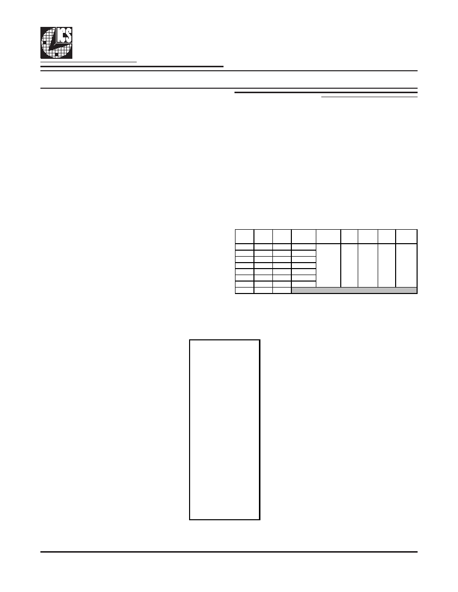
Table 1: CPU Frequency Select Table
FSLC
2
B0b7
FSLB
1
B0b6
FSLA
1
B0b5
CPU
MHz
SRC
MHz
PCI
MHz
REF
MHz
USB
MHz
DOT
MHz
0
266.66
0
1
133.33
0
1
0
200.00
0
1
166.66
1
0
333.33
1
0
1
100.00
1
0
400.00
1
1. FS
LA and FSLB are low-threshold inputs.Pleas e see VIL_FS and VIH_FS specifications in
the Input/Supply/Common Output Parameters Table for correct values.
Also refer to the Test Clarification Table.
2. FS
LC is a three-level input. Please see the VIL_FS and VIH_FS
specifications in the Input/Supply/Common Output Parameters Table for correct values.
Reserved
100.00
33.33
14.318
48.00
96.00
PCI0/CR#_A 1
48 SCLK
VDDPCI 2
47 SDATA
PCI4/SRC5_EN 3
46 REF0/FSLC/TEST_SEL
PCI_F5/ITP_EN 4
45 VDDREF
GNDPCI 5
44 X1
VDD48 6
43 X2
USB_48MHz/FSLA 7
42 GNDREF
GND48 8
41 FSLB/TEST_MODE
VDD96_IO 9
40 CK_PWRGD/PD#
DOT96T_LPR/SRCT0_LPR 10
39 VDDCPU
DOT96C_LPR/SRCC0_LPR 11
38 CPUT0_LPR
GND 12
37 CPUC0_LPR
VDD 13
36 GNDCPU
SE1 14
35 CPUT1_LPR_F
GND 15
34 CPUC1_LPR_F
SRCT2_LPR/SATAT_LPR 16
33 VDDCPU_IO
SRCC2_LPR/SATAC_LPR 17
32 CPUT2_ITP_LPR/SRCT8_LPR
GNDSRC 18
31 CPUC2_ITP_LPR/SRCC8_LPR
SRCT3_LPR/CR#_C 19
30 VDDSRC_IO
SRCC3_LPR/CR#_D 20
29 SRCT7_LPR/CR#_F
VDDSRC_IO 21
28 SRCC7_LPR/CR#_E
SRCT4_LPR 22
27 GNDSRC
SRCC4_LPR 23
26 VDDSRC
CPU_STOP#/SRCC5_LPR 24
25 PCI_STOP#/SRCT5_LPR
48-SSOP/TSSOP
* Internal Pull-Up Resistor
** Internal Pull-Down Resistor
9
L
P
R
S
5
4
5
相關(guān)PDF資料 |
PDF描述 |
|---|---|
| 9173B-01CS08LFT | 75 MHz, VIDEO CLOCK GENERATOR, PDSO8 |
| 951601AFLFT | 66.66 MHz, PROC SPECIFIC CLOCK GENERATOR, PDSO48 |
| 954201BFLFT | 400 MHz, PROC SPECIFIC CLOCK GENERATOR, PDSO56 |
| 935271490512 | 4 CHANNEL(S), 5M bps, SERIAL COMM CONTROLLER, PQCC68 |
| 935271979118 | 8 I/O, PIA-GENERAL PURPOSE, PQCC16 |
相關(guān)代理商/技術(shù)參數(shù) |
參數(shù)描述 |
|---|---|
| 9LPRS552AGLF | 制造商:Integrated Device Technology Inc 功能描述:IDT 9LPRS552AGLF GENERAL PURPOSE SEMICONDUCTORS - Rail/Tube 制造商:Integrated Device Technology Inc 功能描述:IDT 9LPRS552AGLF General Purpose Semiconductors |
| 9LPRS926EGLF | 制造商:Integrated Device Technology Inc 功能描述:IDT 9LPRS926EGLF GENERAL PURPOSE SEMICONDUCTORS - Rail/Tube 制造商:Integrated Device Technology Inc 功能描述:IDT 9LPRS926EGLF General Purpose Semiconductors |
| 9LPRS926EGLFT | 制造商:Integrated Device Technology Inc 功能描述:IDT 9LPRS926EGLFT LOGIC AND TIMING MISC - Tape and Reel 制造商:Integrated Device Technology Inc 功能描述:IDT 9LPRS926EGLFT Logic and Timing Misc |
| 9LQA01241 | 制造商:Denon Electronics 功能描述:REAR PLATE D-M10 |
| 9LQA01441 | 制造商:Denon 功能描述:TOP COVERAVR1600 |
發(fā)布緊急采購(gòu),3分鐘左右您將得到回復(fù)。