- 您現(xiàn)在的位置:買賣IC網(wǎng) > PDF目錄25569 > 9LPR501SGLFT (INTEGRATED DEVICE TECHNOLOGY INC) SPECIALTY MICROPROCESSOR CIRCUIT, PDSO64 PDF資料下載
參數(shù)資料
| 型號: | 9LPR501SGLFT |
| 廠商: | INTEGRATED DEVICE TECHNOLOGY INC |
| 元件分類: | 微控制器/微處理器 |
| 英文描述: | SPECIALTY MICROPROCESSOR CIRCUIT, PDSO64 |
| 封裝: | 6.10 MM, 0.50 MM PITCH, ROHS COMPLIANT, MO-153, TSSOP-64 |
| 文件頁數(shù): | 19/21頁 |
| 文件大小: | 197K |
| 代理商: | 9LPR501SGLFT |

IDTTM/ICSTM
64-pin CK505 w/Fully Integrated Voltage Regulator
1118N—05/19/11
Advance Information
ICS9LPR501
64-PIN CK505 W/FULLY INTEGRATED VOLTAGE REGULATOR
7
Datasheet
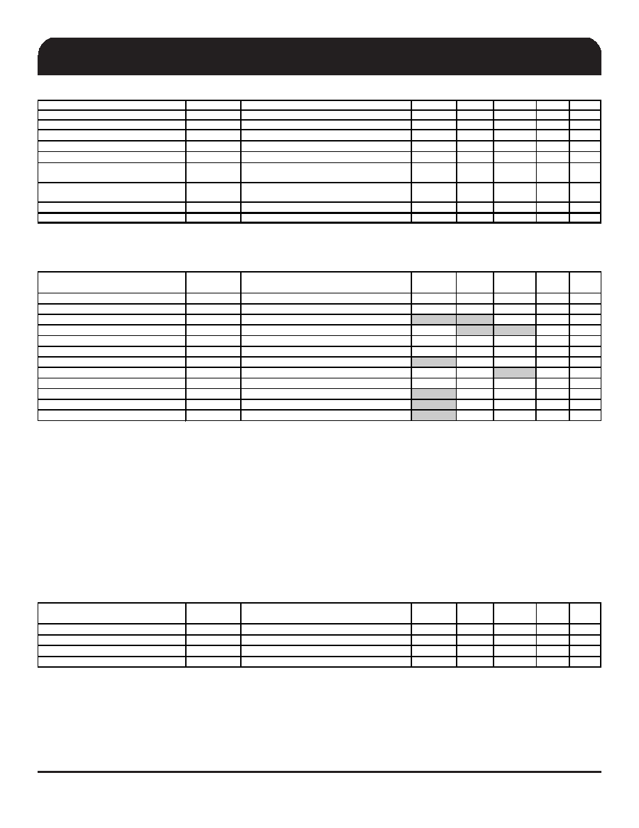
Absolute Maximum Ratings - DC Parameters
PARAMETER
SYMBOL
CONDITIONS
MIN
TYP
M AX
UNITS
Notes
Maximum Supply Voltage
VDDxxx
Supply Voltage4.6
V
7
Maximum Supply Voltage
VDDxxx_IO
Low-Voltage Differential I/ O Supp ly
3.8
V
7
Maximum Input Volt age
VIH
3.3V Inputs
4.6
V
4,5,7
Minimum Input Voltage
VIL
Any Input
GND - 0.5
V
4,7
Case Temperature
Tcase
115
°
C
Thermal Resistance f ro m Die to Ambient
Air
JA
32.5
°C/W
Thermal Resistance from Die to Packag e
Case
JC
68.2
°C/W
Storage Temperature
Ts
-
-65
1 50
°C
4,7
Input ESD protection
ESD p ro t
Hu man Body Model
2000
V
6,7
1Guaranteed by design and characterization, not 100% tested in production.
2 Operation under these conditions is neither implied, nor guaranteed.
3 Maximum input voltage is not to exceed VDD
Clock Jitter Specs - Low Power Differential Outputs
PARAMETER
SYMBOL
CONDITIONS
MIN
TYP
MAX
UNITS NOTES
CPU Jitter - Cycle to Cycle
CPUJC2C
Differential Measurement
58.1
85
ps
1
SRC Jitter - Cycle to Cycle
SRCJC2C
Differential Measurement
36.2
125
ps
1,2
SATA Jitter - Cycle to Cycle
SATAJC2C
Differential Measurement
46.8
125
ps
1
DOT Jitter - Cycle to Cycle
DOTJC2C
Differential Measurement
73.0
250
ps
1
NOTES on DIF Output Jitter: (unless otherwise noted, guaranteed by design and characterization, not 100% tested in production).
1JItter specs are specified as measured on a clock characterization board. System designers need to take special care not to use these numbers, as the in-
system performance will be somewhat degraded. The receiver EMTS (chispet or CPU) will have the receiver jitter specs as measured in a real system.
2 Phase jitter requirement: The SRC outputs will meet the reference clock jitter requiremernts from the PCI Express Gen1 Base Spec. The test is performed on a
component test board under quiet condittions with all outputs on. Jitter analysis is performed using the standardized tool provided by the PCI SIG.
AC Electrical Characteristics - Low Power Differential Outputs
PARAMETER
SYMBOL
CONDITIONS
MIN
TYP
MAX
UNITS NOTES
Rising Edge Slew Rate
tSLR
Averaging on
2.5
3.35
4
V/ns
2, 3
Falling Edge Slew Rate
tFLR
Averaging on
2.5
3.30
4
V/ns
2, 3
Slew Rate Variation
tSLVAR
Averaging on
20
%
1, 10
Differential Voltage Swing
VSWING
Averaging off
300
mV
2
Crossing Point Voltage
VXABS
Averaging off
300
405.5
550
mV
1,4,5
Crossing Point Variation
VXABSVAR
Averaging off
60
140
mV
1,4,9
Maximum Output Voltage
VHIGH
Averaging off
894
1150
mV
1,7
Minimum Output Voltage
VLOW
Averaging off
-300
59.5
mV
1,8
Duty Cycle
DCYC
Averaging on
45
51.0
55
%
2
CPU[1:0] Skew
CPUSKEW10
Differential Measurement
47
100
ps
1
CPU[2_ITP:0] Skew
CPUSKEW20
Differential Measurement
125
150
ps
1
SRC[10:0] Skew
SRCSKEW
Differential Measurement
704
3000
ps
1,6
1Measurement taken for single ended waveform on a component test board (not in system)
2 Measurement taken from differential waveform on a component test board. (not in system)
3 Slew rate emastured through V_swing voltage range centered about differential zero
4 Vcross is defined at the voltage where Clock = Clock#, measured on a component test board (not in system)
9 The total variation of all Vcross measurements in any particular system. Note this is a subset of V_cross min/mas (V_Cross absolute) allowed. The
intent is to limit Vcross induced modulation by setting C_cross_delta to be smaller than V_Cross absolute.
10 Matching applies to rising edge rate for Clock and falling edge rate for Clock#. It is measured using a +/-75mV window centered on the average cross
point where Clock rising meets Clock# falling. The median cross point is used to calculate the voltage thresholds the oscilloscope is to use for the edge
rate calculations.
5 Only applies to the differential rising edge (Clock rising, Clock# falling)
6 Total distributed intentional SRC to SRC skew.
7 The max voltage including overshoot.
8 The min voltage including undershoot.
NOTES on DIF Output AC Specs: (unless otherwise noted, guaranteed by design and characterization, not 100% tested in production).
相關(guān)PDF資料 |
PDF描述 |
|---|---|
| 9LPR501YGT | SPECIALTY MICROPROCESSOR CIRCUIT, PDSO64 |
| 9LPR502YGLFT | SPECIALTY MICROPROCESSOR CIRCUIT, PDSO56 |
| 9LPRS365BKLFT | SPECIALTY MICROPROCESSOR CIRCUIT, PQCC64 |
| 9LPRS365BGLFT | SPECIALTY MICROPROCESSOR CIRCUIT, PDSO64 |
| 9LPRS436CKLF | SPECIALTY MICROPROCESSOR CIRCUIT, PQCC48 |
相關(guān)代理商/技術(shù)參數(shù) |
參數(shù)描述 |
|---|---|
| 9LPR501YGLFT | 制造商:IDT 制造商全稱:Integrated Device Technology 功能描述:64-PIN CK505 W/FULLY INTEGRATED VOLTAGE REGULATOR |
| 9LPR502HGLF | 制造商:Integrated Device Technology Inc 功能描述:PC CLOCK, TSSOP56 - Rail/Tube |
| 9LPR502HGLFT | 制造商:Integrated Device Technology Inc 功能描述:PC CLOCK, TSSOP56 - Rail/Tube |
| 9LPR502SGLF | 功能描述:時鐘合成器/抖動清除器 PC MAIN CLOCK RoHS:否 制造商:Skyworks Solutions, Inc. 輸出端數(shù)量: 輸出電平: 最大輸出頻率: 輸入電平: 最大輸入頻率:6.1 GHz 電源電壓-最大:3.3 V 電源電壓-最小:2.7 V 封裝 / 箱體:TSSOP-28 封裝:Reel |
| 9LPR502SGLFT | 功能描述:時鐘合成器/抖動清除器 PC MAIN CLOCK RoHS:否 制造商:Skyworks Solutions, Inc. 輸出端數(shù)量: 輸出電平: 最大輸出頻率: 輸入電平: 最大輸入頻率:6.1 GHz 電源電壓-最大:3.3 V 電源電壓-最小:2.7 V 封裝 / 箱體:TSSOP-28 封裝:Reel |
發(fā)布緊急采購,3分鐘左右您將得到回復(fù)。