- 您現(xiàn)在的位置:買賣IC網(wǎng) > PDF目錄122717 > 935261475512 (NXP SEMICONDUCTORS) 8 CHANNEL(S), 500K bps, SERIAL COMM CONTROLLER, PQCC84 PDF資料下載
參數(shù)資料
| 型號: | 935261475512 |
| 廠商: | NXP SEMICONDUCTORS |
| 元件分類: | 微控制器/微處理器 |
| 英文描述: | 8 CHANNEL(S), 500K bps, SERIAL COMM CONTROLLER, PQCC84 |
| 封裝: | PLASTIC, MO-047AF, SOT-189-3, LCC-84 |
| 文件頁數(shù): | 56/59頁 |
| 文件大小: | 383K |
| 代理商: | 935261475512 |
第1頁第2頁第3頁第4頁第5頁第6頁第7頁第8頁第9頁第10頁第11頁第12頁第13頁第14頁第15頁第16頁第17頁第18頁第19頁第20頁第21頁第22頁第23頁第24頁第25頁第26頁第27頁第28頁第29頁第30頁第31頁第32頁第33頁第34頁第35頁第36頁第37頁第38頁第39頁第40頁第41頁第42頁第43頁第44頁第45頁第46頁第47頁第48頁第49頁第50頁第51頁第52頁第53頁第54頁第55頁當(dāng)前第56頁第57頁第58頁第59頁
Philips Semiconductors
Product specification
SC28L198
Octal UART for 3.3V and 5V supply voltage
1999 Jan 14
6
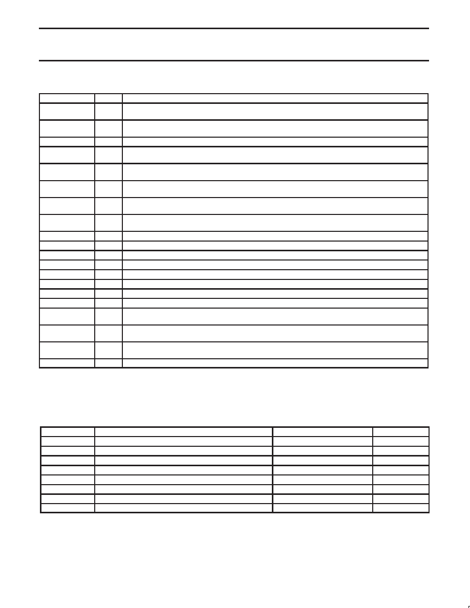
Pin Description
MNEMONIC
TYPE
DESCRIPTION
SClk
I
Host system clock. Used to time operations in the Host Interface and clock internal logic. Must be greater
than twice the frequency of highest X1, Counter/Timer, TxC (1x) or RxC (1x) input frequency.
CEN
I
Chip select: Active low. When asserted, allows I/O access to OCTART registers by host CPU. W_RN signal
indicates direction. (Must not be active in IACKN cycle)
A(7:0)
I
Address lines (A[6] is NOT used. See ”Host Interface” )
D(7:0)
I/O
8–bit bi–directional data bus. Carries command and status information between 28L198 and the host CPU.
Used to convey parallel data for serial I/O between the host CPU and the 28L198
W_RN
I
Write Read not control: When high indicates that the host CPU will write to a 28L198 register or transmit FIFO.
When low, indicates a read cycle. 0 = Read; 1 = Write
DACKN
O
Data Acknowledge: Active low. When asserted, it signals that the last transfer of the D lines is complete.
Open drain.
IRQN
O
Interrupt Request: Active low. When asserted, indicates that the 28L198 requires service for pending inter-
rupt(s). Open drain.
IACKN
I
Interrupt Acknowledge: Active low. When asserted, indicates that the host CPU has initiated an interrupt ac-
knowledge cycle. (Do not use CEN in an IACKN cycle)
TD(a–h)
O
Transmit Data: Serial outputs from the 8 UARTs.
RD(a–h)
I
Receive Data: Serial inputs to the 8 UARTs
I/O0(a–h)
I/O
Input/Output 0: Multi–use input or output pin for the UART.
I/O1(a–h)
I/O
Input/Output 1: Multi–use input or output pin for the UART.
I/O2(a–h)
I/O
Input/Output 2: Multi–use input or output pin for the UART.
I/O3(a–h)
I/O
Input/Output 3: Multi–use input or output pin for the UART.
GIN(1:0)
I
Global general purpose inputs, available to any/all channels.
GOUT0
O
Global general purpose outputs, available from any channel.
RESETN
I
Master reset: Active Low. Must be asserted at power up and may be asserted at other times to reset and re-
start the system. See “Reset Conditions” at end of register map. Minimum width 10 SCLK.
X1/CCLK
I
Crystal 1 or Communication Clock: This pin may be connected to one side of a 2–8 MHz crystal. It may alter-
natively be driven by an external clock in this frequency range. Standard frequency = 3.6864 MHz
X2
O
Crystal 2: If a crystal is used, this is the connection to the second terminal. If a clock signal drives X1, this pin
must be left unconnected.
Power Supplies
I
8 pins total 6 pins for Vss, 2 pins for Vcc
NOTE: Many output pins will have very fast edges, especially when lightly loaded (less than 20 pf.) These edges may move as fast as 1 to 3 ns
fall or rise time. The user must be aware of the possible generation of ringing and reflections on improperly terminated interconnections. See
previous note on Sclk noise under pin assignments.
ABSOLUTE MAXIMUM RATINGS1
SYMBOL
PARAMETER
RATING
UNIT
TA
Operating ambient temperature range2
See Note 3
C
TSTG
Storage temperature range
–65 to +150
C
Vcc
Voltage from VCC to Vss4
–0.5 to +7.0
V
Vss
Voltage from any pin to Vss
–0.5 to Vcc + 0.5
V
PD
Package Power Dissipation (PLCC)
3.78
W
PD
Package Power Dissipation (LQFP)
2.08
W
Derate above 25 C (PLCC pkg.)
30
mW/C
Derate above 25C (LQFP pkg.)
17
mW/C
NOTES:
1. Stresses above those listed under Absolute Maximum Ratings may cause permanent damage to the device. This is a stress rating only and
the functional operation of the device at these or any other conditions above those indicated in the Operation Section of this specification is
not implied.
2. For operating at elevated temperatures, the device must be derated based on +150C maximum junction temperature.
3. Parameters are valid over specified temperature range. See ordering information table for applicable temperature range and operating
supply range.
4. This product includes circuitry specifically designed for the protection of its internal devices from damaging effects of excessive static
charge.
相關(guān)PDF資料 |
PDF描述 |
|---|---|
| 9LPRS365BKLF | SPECIALTY MICROPROCESSOR CIRCUIT, PQCC64 |
| 91W-G28AC-6-CG9 | SINGLE COLOR DISPLAY CLUSTER, GREEN, 7.1 mm |
| 91W-G5AC-6-CW0 | SINGLE COLOR DISPLAY CLUSTER, GREEN, 7.1 mm |
| 94W-EAY2-S0 | SINGLE COLOR LED, AMBER, 8.5 mm |
| 94W-EAY28H-CA0 | SINGLE COLOR LED, AMBER, 8.5 mm |
相關(guān)代理商/技術(shù)參數(shù) |
參數(shù)描述 |
|---|---|
| 935262025112 | 制造商:NXP Semiconductors 功能描述:SUB ONLY IC |
| 935262217118 | 制造商:NXP Semiconductors 功能描述:Real Time Clock Serial 8-Pin SO T/R |
| 935264217557 | 制造商:NXP Semiconductors 功能描述:SUB ONLY IC |
| 935267356112 | 制造商:NXP Semiconductors 功能描述:IC TEA1507PN |
| 935268081112 | 制造商:NXP Semiconductors 功能描述:SUB ONLY IC |
發(fā)布緊急采購,3分鐘左右您將得到回復(fù)。