- 您現(xiàn)在的位置:買賣IC網(wǎng) > PDF目錄36334 > 935260699551 (NXP SEMICONDUCTORS) SPECIALTY CONSUMER CIRCUIT, PQFP208 PDF資料下載
參數(shù)資料
| 型號(hào): | 935260699551 |
| 廠商: | NXP SEMICONDUCTORS |
| 元件分類: | 消費(fèi)家電 |
| 英文描述: | SPECIALTY CONSUMER CIRCUIT, PQFP208 |
| 封裝: | PLASTIC, SOT-316, SQFP-208 |
| 文件頁數(shù): | 12/148頁 |
| 文件大?。?/td> | 692K |
| 代理商: | 935260699551 |
第1頁第2頁第3頁第4頁第5頁第6頁第7頁第8頁第9頁第10頁第11頁當(dāng)前第12頁第13頁第14頁第15頁第16頁第17頁第18頁第19頁第20頁第21頁第22頁第23頁第24頁第25頁第26頁第27頁第28頁第29頁第30頁第31頁第32頁第33頁第34頁第35頁第36頁第37頁第38頁第39頁第40頁第41頁第42頁第43頁第44頁第45頁第46頁第47頁第48頁第49頁第50頁第51頁第52頁第53頁第54頁第55頁第56頁第57頁第58頁第59頁第60頁第61頁第62頁第63頁第64頁第65頁第66頁第67頁第68頁第69頁第70頁第71頁第72頁第73頁第74頁第75頁第76頁第77頁第78頁第79頁第80頁第81頁第82頁第83頁第84頁第85頁第86頁第87頁第88頁第89頁第90頁第91頁第92頁第93頁第94頁第95頁第96頁第97頁第98頁第99頁第100頁第101頁第102頁第103頁第104頁第105頁第106頁第107頁第108頁第109頁第110頁第111頁第112頁第113頁第114頁第115頁第116頁第117頁第118頁第119頁第120頁第121頁第122頁第123頁第124頁第125頁第126頁第127頁第128頁第129頁第130頁第131頁第132頁第133頁第134頁第135頁第136頁第137頁第138頁第139頁第140頁第141頁第142頁第143頁第144頁第145頁第146頁第147頁第148頁
1998 Apr 09
109
Philips Semiconductors
Product specication
Multimedia bridge, high performance
Scaler and PCI circuit (SPCI)
SAA7146A
Table 94 Overview of peak data rates for non-increment (burst) block transfer congurations at 33 MHz PCI clock
Note
1. These peak data rates could be reached for transfers with large BLOCKLENGTH settings, in a well performing
PCI-bus system with low bus load and an appropriate target system without cycle stretching or interrupts.
2. No cycle stretching by RDY/DTACK possible.
PROTOCOL
MODE
TIMEOUT
VALUE
WORD
WIDTH
FAST
MODE
TRANSFER
DIRECTION
TARGET SIDE
PEAK DATA
RATE
OVERALL
PEAK DATA
RATE(1)
Intel/Motorola(2)
0
16 bit
enabled
R/W
33 Mbytes/s
23.0 Mbytes/s
Intel/Motorola(2)
0
8 bit
enabled
R/W
16.5 Mbytes/s
13.5 Mbytes/s
Intel/Motorola
1
16 bit
enabled
R/W
22 Mbytes/s
17.0 Mbytes/s
Intel/Motorola
3
16 bit
enabled
R/W
13.2 Mbytes/s
11.2 Mbytes/s
Intel/Motorola(2)
0
16 bit
disabled
R/W
22 Mbytes/s
17.0 Mbytes/s
Intel/Motorola
1
16 bit
disabled
R/W
16.5 Mbytes/s
13.5 Mbytes/s
It is possible to halt an actual block transfer by external
interrupt. This is achieved by setting the XIRQ_EN bit in
the DEBI_CONFIG register and asserting the GPIO3 pin
input to LOW while an block transfer is active. If the
XRESUME bit is set to 0, this will end the current block
transfer within the next two Dwords. When XRESUME = 1
the transfer will go to a wait state, but the transfer
operation will not end (DEBI_ACTIVE still asserted). When
GPIO3 is de-asserted to HIGH the block transfer will
resume. The contents of DEBI_AD and DEBI_COMMAND
registers are steadily updated on actual address and block
length values during block transfer. Due to this it is
possible to abort the transfer, read back actual status, do
other transfers and resume later with the saved
information. It should be noted that after a Dword aligned
read block transfer (i.e. if
BLOCKLENGTH [1:0] + A16 [1:0] = 4 or A16 [1:0] = 0) the
read back value of the DEBI_AD register points to the
consecutive address of the just filled PCI memory range.
After a Dword unaligned transfer the read back DEBI_AD
value points 1 Dword further (it should be noted that this
also effects the value of the remaining BLOCKLENGTH
after interrupt; A16 target address read back is not effected
by this). RPS is able to react on the GPIO3 pin events.The
16 AD lines are set to 3-state while DEBI is in XIRQ wait
state (XRESUME enabled). To support target devices of
different endian type the swap register has to be
configured.
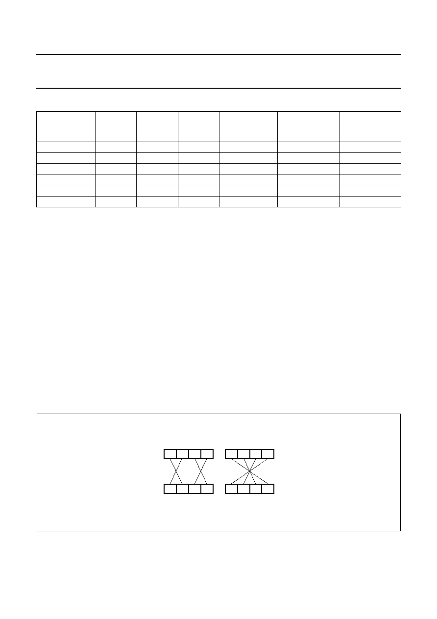
Fig.37 Endian swapping.
handbook, full pagewidth
3210
2301
3210
4-byte swap
the four bytes in a double word
are swapped
2-byte swap
the two bytes in a 2-byte word
are swapped
0123
MHB069
相關(guān)PDF資料 |
PDF描述 |
|---|---|
| 935260699557 | SPECIALTY CONSUMER CIRCUIT, PQFP208 |
| 935243450551 | COLOR SIGNAL ENCODER, PQFP44 |
| 935243450557 | COLOR SIGNAL ENCODER, PQFP44 |
| 935243460551 | COLOR SIGNAL ENCODER, PQFP44 |
| 935243460557 | COLOR SIGNAL ENCODER, PQFP44 |
相關(guān)代理商/技術(shù)參數(shù) |
參數(shù)描述 |
|---|---|
| 935261069122 | 制造商:NXP Semiconductors 功能描述:IC SECURITY TRANSPONDER PLLMC |
| 935262025112 | 制造商:NXP Semiconductors 功能描述:SUB ONLY IC |
| 935262217118 | 制造商:NXP Semiconductors 功能描述:Real Time Clock Serial 8-Pin SO T/R |
| 935264217557 | 制造商:NXP Semiconductors 功能描述:SUB ONLY IC |
| 935267356112 | 制造商:NXP Semiconductors 功能描述:IC TEA1507PN |
發(fā)布緊急采購,3分鐘左右您將得到回復(fù)。