- 您現(xiàn)在的位置:買賣IC網(wǎng) > PDF目錄369342 > 75HVD07 (Texas Instruments, Inc.) MS3420-12 PDF資料下載
參數(shù)資料
| 型號: | 75HVD07 |
| 廠商: | Texas Instruments, Inc. |
| 英文描述: | MS3420-12 |
| 中文描述: | 高輸出RS - 485收發(fā) |
| 文件頁數(shù): | 2/19頁 |
| 文件大小: | 220K |
| 代理商: | 75HVD07 |

SN65HVD05, SN65HVD06, SN65HVD07
SN75HVD05, SN75HVD06, SN75HVD07
SLLS533B
–
MAY 2002
–
REVISED MAY 2003
www.ti.com
2
These devices have imited built-in ESD protection. The eads should be shorted together or the device placed n conductive foam during
storage or handling to prevent electrostatic damage to the MOS gates.
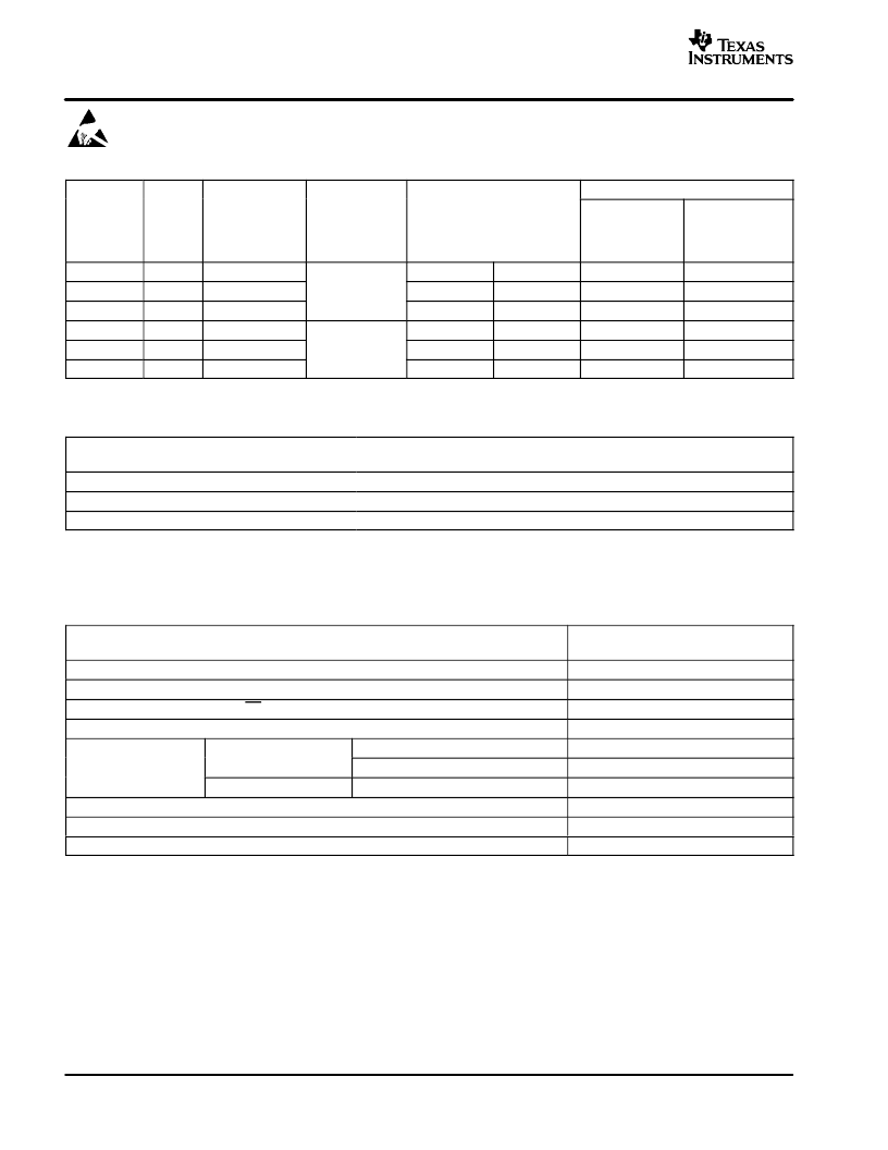
ORDERING INFORMATION
(1)
MARKED AS
SIGNALING
RATE
UNIT
LOAD
DRIVER
OUTPUT SLOPE
CONTROL
TA
PART NUMBER
(2)
PLASTIC
DUAL-IN-LINE
PACKAGE
(PDIP)
65HVD05
SMALL OUTLINE
IC (SOIC)
PACKAGE
40 Mbps
1/2
No
SN65HVD05D
SN65HVD05P
VP05
10 Mbps
1/8
Yes
–
40 C to 85 C
SN65HVD06D
SN65HVD06P
65HVD06
VP06
1 Mbps
1/8
Yes
SN65HVD07D
SN65HVD07P
65HVD07
VP07
40 Mbps
1/2
No
SN75HVD05D
SN75HVD05P
75HVD05
VN05
10 Mbps
1/8
Yes
–
0 C to 70 C
SN75HVD06D
SN75HVD06P
75HVD06
VN06
1 Mbps
1/8
Yes
SN75HVD07D
SN75HVD07P
75HVD07
VN07
(1)For the most current specification and package information, refer to our web site at www.ti.com.
(2)The D package is available taped and reeled. Add an R suffix to the device type (i.e., SN65HVD05DR).
PACKAGE DISSIPATION RATINGS (SEE FIGURE 12 AND FIGURE 13)
TA
≤
25
°
C
POWER RATING
D(2)
710 mW
D(3)
1282 mW
PACKAGE
DERATING FACTOR(1)
ABOVE TA = 25
°
C
5.7 mW/
°
C
10.3 mW/
°
C
8.0 mW/
°
C
TA = 70
°
C
POWER RATING
TA = 85
°
C POWER
RATING
455 mW
369 mW
821 mW
667 mW
P
1000 mW
640 mW
520 mW
(1)This is the inverse of the junction-to-ambient thermal resistance when board-mounted and with no air flow.
(2)Tested in accordance with the Low-K thermal metric definitions of EIA/JESD51-3
(3)Tested in accordance with the High-K thermal metric definitions of EIA/JESD51-7
ABSOLUTE MAXIMUM RATINGS
over operating free-air temperature range unless otherwise noted(1) (2)
SN65HVD05, SN65HVD06, SN65HVD07
SN75HVD05, SN75HVD06, SN75HVD07
Supply voltage range, VCC
Voltage range at A or B
–
0.3 V to 6 V
–
9 V to 14 V
Input voltage range at D, DE, R or RE
Voltage input range, transient pulse, A and B, through 100
(see Figure 11)
–
0.5 V to VCC + 0.5 V
–
50 V to 50 V
Humanbodymodel(3)
Human body model(3)
A, B, and GND
16 kV
Electrostatic discharge
All pins
4 kV
Charged-device model(4)
All pins
1 kV
Continuous total power dissipation
See Dissipation Rating Table
–
65
°
C to 150
°
C
260
°
C
Storage temperature range, Tstg
Lead temperature 1,6 mm (1/16 inch) from case for 10 seconds
(1)Stresses beyond those listed under
“
absolute maximum ratings
”
may cause permanent damage to the device. These are stress ratings only, and
functional operation of the device at these or any other conditions beyond those indicated under
“
recommended operating conditions
”
is not
implied. Exposure to absolute-maximum-rated conditions for extended periods may affect device reliability.
(2)All voltage values, except differential I/O bus voltages, are with respect to network ground terminal.
(3)Tested in accordance with JEDEC Standard 22, Test Method A114-A.
(4)Tested in accordance with JEDEC Standard 22, Test Method C101.
相關(guān)PDF資料 |
PDF描述 |
|---|---|
| 75N75 | 75Amps, 75Volts N-CHANNEL POWER MOSTFET |
| 75N75L-TA3-R | 75Amps, 75Volts N-CHANNEL POWER MOSTFET |
| 75N75L-TA3-T | 75Amps, 75Volts N-CHANNEL POWER MOSTFET |
| 75N75L-TF3-R | 75Amps, 75Volts N-CHANNEL POWER MOSTFET |
| 75N75L-TF3-T | 75Amps, 75Volts N-CHANNEL POWER MOSTFET |
相關(guān)代理商/技術(shù)參數(shù) |
參數(shù)描述 |
|---|---|
| 75IF14X284U | 制造商:Siemens 功能描述: |
| 75-II | 制造商:Fluke Electronics 功能描述: |
| 75II3100AA00K | 制造商:KEMET Corporation 功能描述:METALLIZED POLYPROPYLENE FILM CAPACITOR D.C. AND PULSE APPLICATIONS |
| 75II3120CK30K | 制造商:KEMET Corporation 功能描述:Cap Film 0.12uF 250V PP 10% (18 X 5 X 11mm) Radial 15mm 105 制造商:KEMET Corporation 功能描述:Cap Film 0.12uF 250V PP 10% (18 X 5 X 11mm) Radial 15mm 105°C T/R |
| 75II3180JE40J | 制造商:KEMET Corporation 功能描述:0,18 U 250V 制造商:KEMET Corporation 功能描述:CAP METAL POLY - Bulk |
發(fā)布緊急采購,3分鐘左右您將得到回復(fù)。