- 您現(xiàn)在的位置:買賣IC網(wǎng) > PDF目錄369342 > 75HVD07 (Texas Instruments, Inc.) MS3420-12 PDF資料下載
參數(shù)資料
| 型號(hào): | 75HVD07 |
| 廠商: | Texas Instruments, Inc. |
| 英文描述: | MS3420-12 |
| 中文描述: | 高輸出RS - 485收發(fā) |
| 文件頁數(shù): | 1/19頁 |
| 文件大小: | 220K |
| 代理商: | 75HVD07 |

SN65HVD05, SN65HVD06, SN65HVD07
SN75HVD05, SN75HVD06, SN75HVD07
SLLS533B – MAY 2002 – REVISED MAY 2003
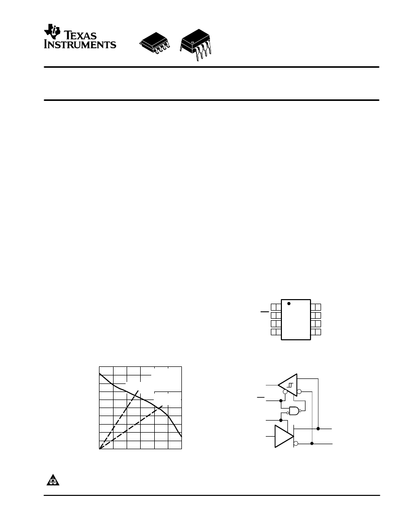
HIGH OUTPUT RS-485 TRANSCEIVERS
FEATURES
Minimum Differential Output Voltage of 2.5 V
Into a 54-
Load
Open-Circuit, Short-Circuit, and Idle-Bus
Failsafe Receiver
1/8
th
Unit-Load Option Available (Up to 256
Nodes on the Bus)
Bus-Pin ESD Protection Exceeds 16 kV HBM
Driver Output Slew Rate Control Options
Electrically Compatible With ANSI
TIA/EIA-485-A Standard
Low-Current Standby Mode
. . .
1
μ
A Typical
Glitch-Free Power-Up and Power-Down
Protection for Hot-Plugging Applications
Pin Compatible With Industry Standard
SN75176
APPLICATIONS
Data Transmission Over Long or Lossy Lines
or Electrically Noisy Environments
Profibus Line Interface
Industrial Process Control Networks
Point-of-Sale (POS) Networks
Electric Utility Metering
Building Automation
Digital Motor Control
DESCRIPTION
The
SN75HVD06, SN65HVD07, and SN75HVD07 combine
a 3-state differential line driver and differential line
receiver. They are designed for balanced data
transmission
and
interoperate
TIA/EIA-485-A and ISO 8482E standard-compliant
devices. The driver is designed to provide a differential
output voltage greater than that required by these
standards for increased noise margin. The drivers and
receivers have active-high and active-low enables
respectively, which can be externally connected
together to function as direction control.
SN65HVD05,
SN75HVD05,
SN65HVD06,
with
ANSI
The driver differential outputs and receiver differential
inputs connect internally to form a differential input/
output (I/O) bus port that is designed to offer minimum
loading to the bus whenever the driver is disabled or not
powered. These devices feature wide positive and
negative common-mode voltage ranges, making them
suitable for party-line applications.
1
2
3
4
8
7
6
5
R
RE
DE
D
V
CC
B
A
GND
D OR P PACKAGE
(TOP VIEW)
0
0.5
1
1.5
2
2.5
3
3.5
4
4.5
5
0
20
40
60
80
100
120
–
DIFFERENTIAL OUTPUT VOLTAGE
vs
DIFFERENTIAL OUTPUT CURRENT
VO
IOD – Differential Output Current – mA
60
Load
Line
30
Load
Line
TA = 25
°
C
DE at VCC
D at VCC
VCC = 5 V
1
2
3
4
6
7
A
B
R
RE
DE
D
LOGIC DIAGRAM
(POSITIVE LOGIC)
PRODUCTION DATA information is current as of publication date. Products
conform to specifications per the terms of Texas Instruments standard warranty.
Production processing does not necessarily include testing of all parameters.
Please be aware that an important notice concerning availability, standard warranty, and use in critical applications of Texas Instruments
semiconductor products and disclaimers thereto appears at the end of this data sheet.
www.ti.com
Copyright
2002–2003, Texas Instruments Incorporated
相關(guān)PDF資料 |
PDF描述 |
|---|---|
| 75N75 | 75Amps, 75Volts N-CHANNEL POWER MOSTFET |
| 75N75L-TA3-R | 75Amps, 75Volts N-CHANNEL POWER MOSTFET |
| 75N75L-TA3-T | 75Amps, 75Volts N-CHANNEL POWER MOSTFET |
| 75N75L-TF3-R | 75Amps, 75Volts N-CHANNEL POWER MOSTFET |
| 75N75L-TF3-T | 75Amps, 75Volts N-CHANNEL POWER MOSTFET |
相關(guān)代理商/技術(shù)參數(shù) |
參數(shù)描述 |
|---|---|
| 75IF14X284U | 制造商:Siemens 功能描述: |
| 75-II | 制造商:Fluke Electronics 功能描述: |
| 75II3100AA00K | 制造商:KEMET Corporation 功能描述:METALLIZED POLYPROPYLENE FILM CAPACITOR D.C. AND PULSE APPLICATIONS |
| 75II3120CK30K | 制造商:KEMET Corporation 功能描述:Cap Film 0.12uF 250V PP 10% (18 X 5 X 11mm) Radial 15mm 105 制造商:KEMET Corporation 功能描述:Cap Film 0.12uF 250V PP 10% (18 X 5 X 11mm) Radial 15mm 105°C T/R |
| 75II3180JE40J | 制造商:KEMET Corporation 功能描述:0,18 U 250V 制造商:KEMET Corporation 功能描述:CAP METAL POLY - Bulk |
發(fā)布緊急采購(gòu),3分鐘左右您將得到回復(fù)。