- 您現(xiàn)在的位置:買(mǎi)賣(mài)IC網(wǎng) > PDF目錄360515 > 7531GROUP 250MA CMOS LDO, ISUPPLY 1UA & 2% VOUT ACCURACY, -40C to +125C, 3-SOT-89, T/R PDF資料下載
參數(shù)資料
| 型號(hào): | 7531GROUP |
| 英文描述: | 250MA CMOS LDO, ISUPPLY 1UA & 2% VOUT ACCURACY, -40C to +125C, 3-SOT-89, T/R |
| 中文描述: | 單芯片8位CMOS微機(jī) |
| 文件頁(yè)數(shù): | 21/64頁(yè) |
| 文件大小: | 633K |
| 代理商: | 7531GROUP |
第1頁(yè)第2頁(yè)第3頁(yè)第4頁(yè)第5頁(yè)第6頁(yè)第7頁(yè)第8頁(yè)第9頁(yè)第10頁(yè)第11頁(yè)第12頁(yè)第13頁(yè)第14頁(yè)第15頁(yè)第16頁(yè)第17頁(yè)第18頁(yè)第19頁(yè)第20頁(yè)當(dāng)前第21頁(yè)第22頁(yè)第23頁(yè)第24頁(yè)第25頁(yè)第26頁(yè)第27頁(yè)第28頁(yè)第29頁(yè)第30頁(yè)第31頁(yè)第32頁(yè)第33頁(yè)第34頁(yè)第35頁(yè)第36頁(yè)第37頁(yè)第38頁(yè)第39頁(yè)第40頁(yè)第41頁(yè)第42頁(yè)第43頁(yè)第44頁(yè)第45頁(yè)第46頁(yè)第47頁(yè)第48頁(yè)第49頁(yè)第50頁(yè)第51頁(yè)第52頁(yè)第53頁(yè)第54頁(yè)第55頁(yè)第56頁(yè)第57頁(yè)第58頁(yè)第59頁(yè)第60頁(yè)第61頁(yè)第62頁(yè)第63頁(yè)第64頁(yè)
SINGLE-CHIP 8-BIT CMOS MICROCOMPUTER
7531 Group
MITSUBISHI MICROCOMPUTERS
21
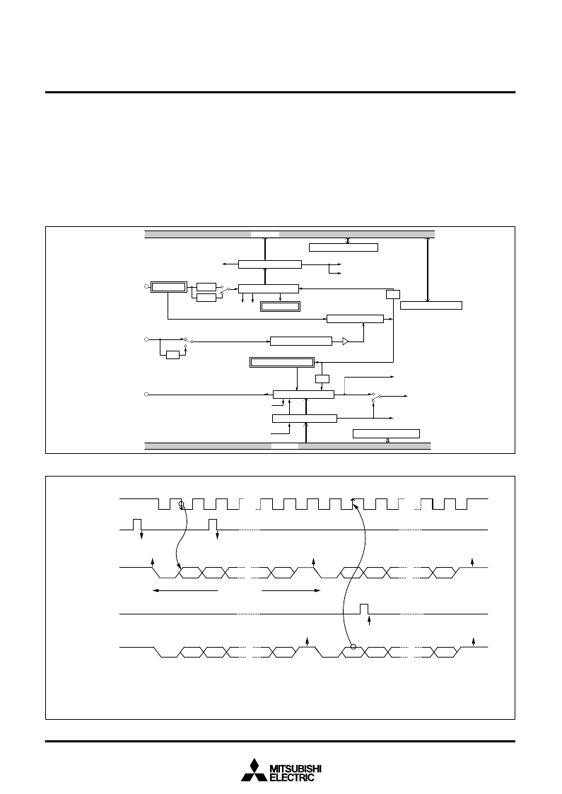
Fig. 23 Block diagram of UART serial I/O
Fig. 24 Operation of UART serial I/O function
Serial I/O
G
Serial I/O1
Serial I/O1 can be used as an asynchronous (UART) serial I/O. A
dedicated timer (baud rate generator) is also provided for baud rate
generation when serial I/O1 is in operation.
Eight serial data transfer formats can be selected, and the transfer
formats to be used by a transmitter and a receiver must be identical.
Each of the transmit and receive shift registers has a buffer register
(the same address on memory). Since the shift register cannot be
written to or read from directly, transmit data is written to the transmit
buffer, and receive data is read from the respective buffer registers.
These buffer registers can also hold the next data to be transmitted
and receive 2-byte receive data in succession.
By selecting “1” for continuous transmit valid bit (bit 2 of SIO1CON),
continuous transmission of the same data is made possible.
This can be used as a simplified PWM.
OE
PE FE
1/16
X
IN
1/4
1/16
Data bus
Receive Buffer Register
Address
(0018
16
)
Receive Shift Register
Receive buffer full flag (RBF)
Receive interrupt request (RI)
ST Detector
SP Detector
UART Control Register
Address (001B
16
)
Address (001A
16
)
Character length selection bit
7-bit
8-bit
Clock Control Circuit
Baud Rate Generator
Address (001C
16
)
Division ratio 1/(n+1)
BRG count source selection bit
Transmit Buffer Register
Data bus
Transmit Shift Register
Address
(0018
16
)
Transmit shift register shift
completion flag (TSC)
Transmit buffer empty flag (TBE)
Transmit interrupt request (TI)
Address (0019
16
)
Character length selection bit
Transmit interrupt source selection bit
Continuous transmit valid bit
Serial I/O1 control register
P1
0
/R
X
D
P1
1
/T
X
D
Serial I/O1 status register
ST/SP/PA Generator
TSC=0
TBE=1
RBF=0
TBE=0
TBE=0
RBF=1
RBF=1
ST
D
0
D
1
SP
D
0
D
1
ST
SP
TBE=1
TSC=1*
ST
D
0
D
1
SP
D
0
D
1
ST
SP
1 :
Error flag detection occurs at the same time that the RBF flag becomes “1” (at 1st stop bit, during reception).
2 :
The transmit interrupt (TI) can be selected to occur when either the TBE or TSC flag becomes “1”, depending on the setting of the transmit
interrupt source selection bit (TIC) of the serial I/O1 control register.
3 :
The receive interrupt (RI) is set when the RBF flag becomes “1”.
4 :
After data is written to the transmit buffer when TSC = 1, 0.5 to 1.5 cycles of the data shift cycle is necessary until changing to TSC = 0.
Notes
Transmit/Receive Clock
Transmit Buffer Register
Write Signal
Serial Output T
X
D
Receive Buffer Register
Read Signal
Serial Input R
X
D
* Generated at second bit in 2-stop -bit
mode
1 Start Bit
7 or 8 Data Bit
1 or 0 Parity Bit
1 or 2 Stop Bit
相關(guān)PDF資料 |
PDF描述 |
|---|---|
| 7531 | 250mA CMOS LDO, Isupply 1uA and 2% Vout Accuracy, -40C to +125C, 3-SOT-23, T/R |
| 7532 | Low Quiescent Current LDO, -40C to +125C, 3-SOT-23, T/R |
| 7533 | 250mA CMOS LDO, lsupply 1uA and 2% Vout Accuracy, -40C to +125C, 3-SOT-23, T/R |
| 753252 | 250mA CMOS LDO, lsupply 1uA and 2% Vout Accuracy, -40C to +125C, 3-SOT-23, T/R |
| 7535 | Low Quiescent Current LDO, -40C to +125C, 3-SOT-23, T/R |
相關(guān)代理商/技術(shù)參數(shù) |
參數(shù)描述 |
|---|---|
| 7532 | 制造商:BM Connecting Cables 功能描述:T/STONE G KVLR GLVS 9 |
| 7532/7536 | 制造商:未知廠(chǎng)家 制造商全稱(chēng):未知廠(chǎng)家 功能描述:7532/7536 Group USER'S MANUALHardware Manual & Device User's Manual 1715K/SEP.05.00 |
| 75320 | 功能描述:BIT MICRO HEX SYST4 2.0MM 28MM RoHS:否 類(lèi)別:工具 >> 螺釘和螺母驅(qū)動(dòng)器 - 刀片和位 系列:系統(tǒng) 4 標(biāo)準(zhǔn)包裝:1 系列:TorqueVario™ 類(lèi)型:十字槽刀片 尺寸:#2 長(zhǎng)度:7.48"(190mm) 特點(diǎn):絕緣達(dá) 10,000V 重量:0.07 磅(31.75g) |
| 753201102GP | 制造商:CTS Corporation 功能描述:RES NET 1K OHM 2% 17/25W 200PPM/ C BUS 20PIN DUAL ROW SMD - Bulk |
| 753201102GPTR13 | 制造商:CTS Corporation 功能描述:RES NET 1K OHM 2% 17/25W 200PPM/ C BUS 20PIN DUAL ROW SMD - Tape and Reel |
發(fā)布緊急采購(gòu),3分鐘左右您將得到回復(fù)。