- 您現(xiàn)在的位置:買賣IC網 > PDF目錄68811 > 71M6532F-IGTR/F (MAXIM INTEGRATED PRODUCTS INC) 1-CHANNEL POWER SUPPLY MANAGEMENT CKT, PQFP100 PDF資料下載
參數資料
| 型號: | 71M6532F-IGTR/F |
| 廠商: | MAXIM INTEGRATED PRODUCTS INC |
| 元件分類: | 電源管理 |
| 英文描述: | 1-CHANNEL POWER SUPPLY MANAGEMENT CKT, PQFP100 |
| 封裝: | LEAD FREE, LQFP-100 |
| 文件頁數: | 60/120頁 |
| 文件大?。?/td> | 2477K |
| 代理商: | 71M6532F-IGTR/F |
第1頁第2頁第3頁第4頁第5頁第6頁第7頁第8頁第9頁第10頁第11頁第12頁第13頁第14頁第15頁第16頁第17頁第18頁第19頁第20頁第21頁第22頁第23頁第24頁第25頁第26頁第27頁第28頁第29頁第30頁第31頁第32頁第33頁第34頁第35頁第36頁第37頁第38頁第39頁第40頁第41頁第42頁第43頁第44頁第45頁第46頁第47頁第48頁第49頁第50頁第51頁第52頁第53頁第54頁第55頁第56頁第57頁第58頁第59頁當前第60頁第61頁第62頁第63頁第64頁第65頁第66頁第67頁第68頁第69頁第70頁第71頁第72頁第73頁第74頁第75頁第76頁第77頁第78頁第79頁第80頁第81頁第82頁第83頁第84頁第85頁第86頁第87頁第88頁第89頁第90頁第91頁第92頁第93頁第94頁第95頁第96頁第97頁第98頁第99頁第100頁第101頁第102頁第103頁第104頁第105頁第106頁第107頁第108頁第109頁第110頁第111頁第112頁第113頁第114頁第115頁第116頁第117頁第118頁第119頁第120頁
Data Sheet 71M6531D/F-71M6532D/F
FDS 6531/6532 005
44
2005-2010 TERIDIAN Semiconductor Corporation
v1.3
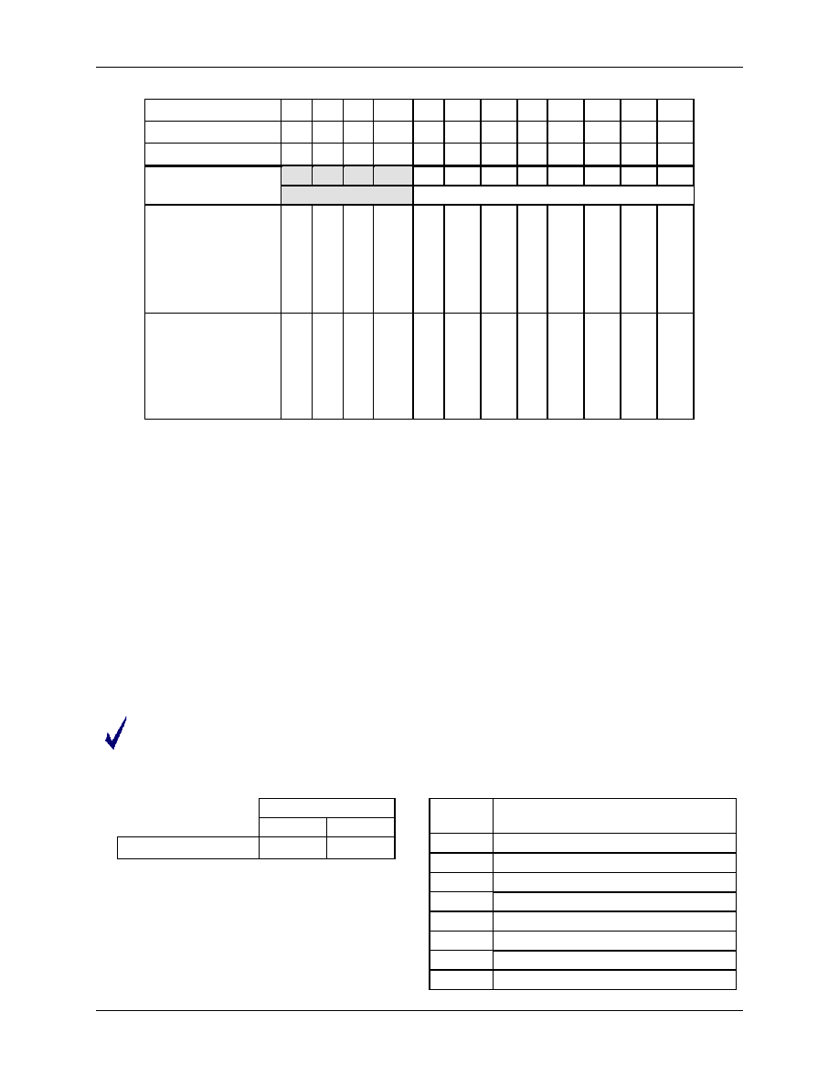
Table 44: Data/Direction Registers and Internal Resources for DIO 40-51 (71M6532D/F)
DIO
40
41
42
43
44
45
–
47
48
49
50
51
LCD Segment
60
61
62
63
64
65
–
67
68
69
70
71
Pin number
95
97
98
40
31
38
–
22
23
24
25
50
Configuration (DIO
or LCD segment)
4
5
6
7
0
1
–
3
4
5
6
7
LCD_BITMAP[63:56]
LCD_BITMAP[71:64]
Data Register
L
C
D_S
E
G60[
0]
L
C
D_S
E
G61[
0]
L
C
D_S
E
G62[
0]
L
C
D_S
E
G63[
0]
L
C
D_S
E
G64[
0]
L
C
D_S
E
G65[
0]
–
L
C
D_S
E
G67[
0]
L
C
D_S
E
G68[
0]
L
C
D_S
E
G69[
0]
L
C
D_S
E
G70[
0]
L
C
D_S
E
G71[
0]
Direction Register
0 = input,
1 = output
L
C
D_S
E
G60[
0]
L
C
D_S
E
G61[
0]
L
C
D_S
E
G62[
0]
L
C
D_S
E
G63[
0
]
L
C
D_S
E
G64[
3]
L
C
D_S
E
G65[
3]
–
L
C
D_S
E
G67[
3]
L
C
D_S
E
G68[
3]
L
C
D_S
E
G69[
3]
L
C
D_S
E
G70[
3]
L
C
D_S
E
G71[
3]
DIO24 and higher do not have SFR registers for direction control. DIO40 and higher do not have SFR
registers for data access. The direction control of these pins is achieved with the LCD_SEGn[3] bits and
data access is controlled with the LCD_SEGn[0] bits in I/O RAM.
DIO56 through DIO58 are dedicated DIO pins. They are controlled with DIO_DIR56[7] through
DIO_DIR58[7] and with DIO_56[4] through DIO_58[4] in I/O RAM.
1.5.9
Digital IO – Common Characteristics for 71M6531D/F and 71M6532D/F
On reset or power-up, all DIO pins are inputs until they are configured for the desired direction under
MPU control. The pin function can be configured by the I/O RAM bits LCD_BITMAPn. Setting
LCD_BITMAPn = 1 configures the pin for LCD, setting LCD_BITMAPn = 0 configures it for DIO. Once a
pin is configured as DIO, it can be configured independently as an input or output with the DIO_DIR bits
or the LCD_SEGn registers. Input and output data are written to or read from the pins using SFR registers
P0, P1, and P2.
DIO24 and higher do not have SFR registers for direction control. DIO40 and higher do not have SFR
registers for data access. The direction control of these pins is achieved with the LCD_SEGn[3] registers
and data access is controlled with the LCD_SEGn[0] registers in I/O RAM.
Since the control for DIO24 through DIO51 is shared with the control for LCD segments, the firmware
must take care not to disturb the DIO pins when accessing the LCD segments and vice versa. Usually,
this requires reading the I/O RAM register, applying a mask and writing back the modified byte.
Table 45: DIO_DIR Control Bit
DIO_DIR [n]
0
1
DIO Pin n Function
Input
Output
Table 46: Selectable Control using DIO_DIR Bits
DIO_R
Value
Resource Selected for DIO Pin
0
None
1
Reserved
2
T0 (counter 0 clock)
3
T1 (counter 1 clock)
4
High priority I/O interrupt (INT0 rising)
5
Low priority I/O interrupt (INT1 rising)
6
High priority I/O interrupt (INT0 falling)
7
Low priority I/O interrupt (INT1 falling)
相關PDF資料 |
PDF描述 |
|---|---|
| 71M6534-IGT/F | SPECIALTY ANALOG CIRCUIT, PQFP120 |
| 71M6534H-IGTR/F | SPECIALTY ANALOG CIRCUIT, PQFP120 |
| 71M6533H-IGTR/F | SPECIALTY ANALOG CIRCUIT, PQFP100 |
| 71M6534-IGTR/F | SPECIALTY ANALOG CIRCUIT, PQFP120 |
| 71M6534H-IGT/F | SPECIALTY ANALOG CIRCUIT, PQFP120 |
相關代理商/技術參數 |
參數描述 |
|---|---|
| 71M6533 | 制造商:TERIDIAN 制造商全稱:TERIDIAN 功能描述:Energy Meter IC |
| 71M6533-DB | 功能描述:開發(fā)板和工具包 - 8051 71M6533 Demo Brd RoHS:否 制造商:Silicon Labs 產品:Development Kits 工具用于評估:C8051F960, Si7005 核心: 接口類型:USB 工作電源電壓: |
| 71M6533G | 制造商:MAXIM 制造商全稱:Maxim Integrated Products 功能描述:Exceeds IEC 62053/ANSI C12.20 Standards |
| 71M6533G-IGTR/F | 功能描述:計量片上系統(tǒng) - SoC AC Power Monitoring SoC-Programd RoHS:否 制造商:Maxim Integrated 核心:80515 MPU 處理器系列:71M6511 類型:Metering SoC 最大時鐘頻率:70 Hz 程序存儲器大小:64 KB 數據 RAM 大小:7 KB 接口類型:UART 可編程輸入/輸出端數量:12 片上 ADC: 安裝風格:SMD/SMT 封裝 / 箱體:LQFP-64 封裝:Reel |
| 71M6533H | 制造商:TERIDIAN 制造商全稱:TERIDIAN 功能描述:Energy Meter IC |
發(fā)布緊急采購,3分鐘左右您將得到回復。