- 您現(xiàn)在的位置:買賣IC網(wǎng) > PDF目錄371400 > 24WC02 1K/2K/4K/8K/16K-Bit Serial E2PROM PDF資料下載
參數(shù)資料
| 型號: | 24WC02 |
| 英文描述: | 1K/2K/4K/8K/16K-Bit Serial E2PROM |
| 中文描述: | 1K/2K/4K/8K/16K-Bit串行E2PROM |
| 文件頁數(shù): | 1/9頁 |
| 文件大?。?/td> | 45K |
| 代理商: | 24WC02 |

1
CAT24WC01/02/04/08/16
1K/2K/4K/8K/16K-Bit Serial E
2
PROM
* Catalyst Semiconductor is licensed by Philips Corporation to carry the I
2
C Bus Protocol.
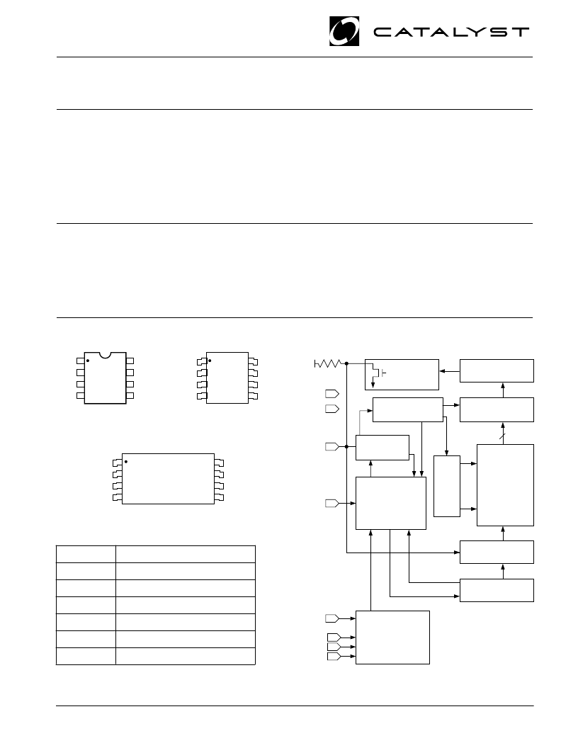
PIN CONFIGURATION
DIP Package (P)
BLOCK DIAGRAM
PIN FUNCTIONS
Pin Name
Function
A0, A1, A2
Device Address Inputs
SDA
Serial Data/Address
SCL
Serial Clock
WP
Write Protect
V
CC
+1.8V to +6.0V Power Supply
V
SS
Ground
24WCXX F03
SOIC Package (J)
5020 FHD F01
FEATURES
I
400 KHZ I
2
C Bus Compatible*
I
1.8 to 6.0Volt Operation
I
Low Power CMOS Technology
I
Write Protect Feature
— Entire Array Protected When WP at V
IH
I
Page Write Buffer
DESCRIPTION
I
Self-Timed Write Cycle with Auto-Clear
I
1,000,000 Program/Erase Cycles
I
100 Year Data Retention
I
8-pin DIP, 8-pin SOIC or 8 pin TSSOP
I
Commercial, Industrial and Automotive
Temperature Ranges
The CAT24WC01/02/04/08/16 is a 1K/2K/4K/8K/16K-
bit Serial CMOS E
2
PROM internally organized as 128/
256/512/1024/2048 words of 8 bits each. Catalyst’s
advanced CMOS technology substantially reduces de-
vice power requirements. The the CAT24WC01/02/04/
08/16 feature a 16-byte page write buffer. The device
operates via the I
2
C bus serial interface, has a special
write protection feature, and is available in 8-pin DIP, 8-
pin SOIC or 8-pin TSSOP.
1999 by Catalyst Semiconductor, Inc.
Characteristics subject to change without notice
8
7
6
5
VCC
WP
SCL
SDA
A2
A0
A1
VSS
1
2
3
4
TSSOP Package (U)
(* Available for 24WC01 and 24WC02 only)
DOUT
ACK
SENSE AMPS
SHIFT REGISTERS
CONTROL
LOGIC
WORD ADDRESS
BUFFERS
START/STOP
LOGIC
STATE COUNTERS
SLAVE
ADDRESS
COMPARATORS
E
2
PROM
VCC
EXTERNAL LOAD
COLUMN
DECODERS
XDEC
DATA IN STORAGE
HIGH VOLTAGE/
TIMING CONTROL
VSS
WP
SCL
A0
A1
A2
SDA
A2
A0
A1
VSS
1
2
3
4
8
7
6
5
VCC
WP
SCL
SDA
A0
A1
A2
VCC
WP
SCL
SDA
1
2
3
4
8
7
6
5
VSS
Doc. No. 25051-00 3/98 S-1
相關(guān)PDF資料 |
PDF描述 |
|---|---|
| 24WC16 | 1K/2K/4K/8K/16K-Bit Serial E2PROM |
| 24WC128 | 64K 8K x 8 Battery-Voltage CMOS E2PROM |
| 24WC32 | 64K 8K x 8 Battery-Voltage CMOS E2PROM |
| 250-8501-010 | Low-Power, SPST, Fast, CMOS Analog Switch |
| 2500-10J | Molded Unshielded RF Coils |
相關(guān)代理商/技術(shù)參數(shù) |
參數(shù)描述 |
|---|---|
| 24WC128 | 制造商:CATALYST 制造商全稱:Catalyst Semiconductor 功能描述:128K-Bit I2C Serial CMOS E2PROM |
| 24WC16 | 制造商:CATALYST 制造商全稱:Catalyst Semiconductor 功能描述:1K/2K/4K/8K/16K-Bit Serial E2PROM |
| 24WC256KI | 制造商:CSI 功能描述: |
| 24WC32 | 制造商:CATALYST 制造商全稱:Catalyst Semiconductor 功能描述:32K/64K-Bit I2C Serial CMOS E2PROM |
| 24WC32P | 制造商:CATALYST 功能描述: |
發(fā)布緊急采購,3分鐘左右您將得到回復(fù)。