- 您現(xiàn)在的位置:買賣IC網(wǎng) > PDF目錄16512 > XR19L210IL40-0B-EB (Exar Corporation)EVAL BOARD FOR XR19L202 40QFN PDF資料下載
參數(shù)資料
| 型號(hào): | XR19L210IL40-0B-EB |
| 廠商: | Exar Corporation |
| 文件頁數(shù): | 34/43頁 |
| 文件大小: | 0K |
| 描述: | EVAL BOARD FOR XR19L202 40QFN |
| 標(biāo)準(zhǔn)包裝: | 1 |
| 系列: | * |
第1頁第2頁第3頁第4頁第5頁第6頁第7頁第8頁第9頁第10頁第11頁第12頁第13頁第14頁第15頁第16頁第17頁第18頁第19頁第20頁第21頁第22頁第23頁第24頁第25頁第26頁第27頁第28頁第29頁第30頁第31頁第32頁第33頁當(dāng)前第34頁第35頁第36頁第37頁第38頁第39頁第40頁第41頁第42頁第43頁

XR19L210
4
SINGLE CHANNEL INTEGRATED UART AND RS-232 TRANSCEIVER
REV. 1.0.2
NOTE: Pin type: I=Input, O=Output, I/O= Input/output, OD=Output Open Drain. For CMOS/TTL Voltage levels, ’LOW’
indicates a voltage in the range 0V to VIL and ’HIGH" indicates a voltage in the range VIH to VCC. For RS-232
input voltage levels, ’LOW’ is any voltage < -3V and ’HIGH’ is any voltage > 3V. For RS-232 output voltage levels,
’LOW’ is any voltage < -5V and ’HIGH’ is any voltage > 5V.
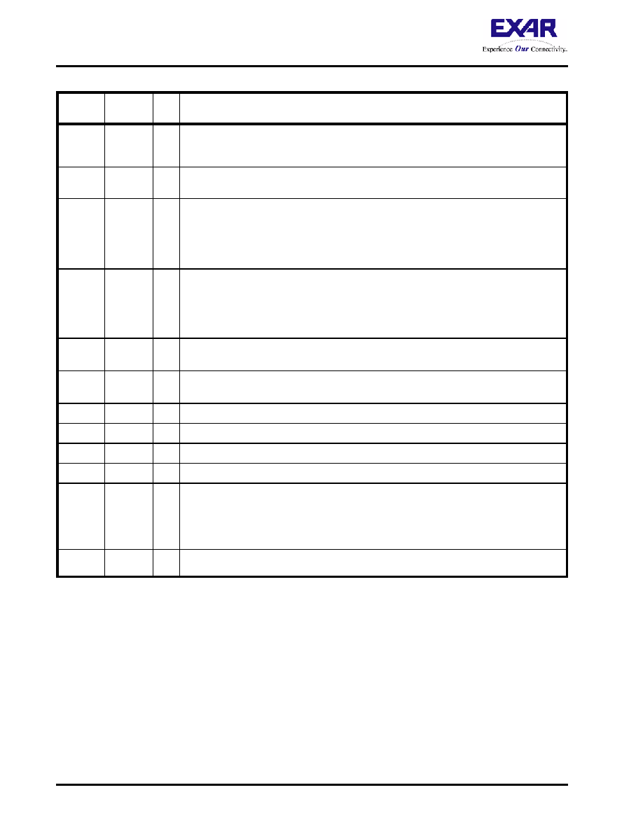
PwrSave
13
I
Power-Save (active high). This feature isolates the L210’s data bus interface from the host
preventing other bus activities that cause higher power drain during sleep mode. See Sleep
Mode with Auto Wake-up and Power-Save Feature section for details.
ACP
16
I
Autosleep for Charge Pump (active HIGH). When this pin is HIGH, the charge pump is shut
off if the L210 is already in partial sleep mode, i.e. the crystal oscillator is stopped.
I/M#
4
I
Intel or Motorola Bus Select.
When I/M# pin is HIGH, 16 or Intel Mode, the device will operate in the Intel bus type of
interface.
When I/M# pin is LOW, 68 or Motorola mode, the device will operate in the Motorola bus
type of interface.
RESET
(RESET#)
28
I
When I/M# pin is HIGH for Intel bus interface, this input becomes RESET (active high).
When I/M# pin is LOW for Motorola bus interface, this input becomes RESET# (active low).
A 40 ns minimum active pulse on this pin will reset the internal registers and all outputs of
the UART. The UART transmitter output will be held HIGH, the receiver input will be ignored
and outputs are reset during reset period (see
C2+
C2-
20
21
-
Charge pump capacitors. As shown in
Figure 1, a 0.1 uF capacitor should be placed
between these 2 pins.
C1+
C1-
29
30
-
Charge pump capacitors. As shown in
Figure 1, a 0.1 uF capacitor should be placed
between these 2 pins.
VREF+
32
Pwr +5.0V generated by the charge pump.
VREF-
22
Pwr -5.0V generated by the charge pump.
VCC
33
Pwr 3.0V to 5.5V power supply. All CMOS/TTL input pins, except XTAL1, are 5V tolerant.
GND
6, 18, 27
Pwr Power supply common, ground.
-
PAD
Pwr The center pad on the backside of the 40-QFN package is metallic and is not electrically
connected to anything inside the device. It must be soldered on to the PCB and may be
optionally connected to GND on the PCB. The thermal pad size on the PCB should be the
approximate size of this center pad and should be solder mask defined. The solder mask
opening should be at least 0.0025" inwards from the edge of the PCB thermal pad.
NC
3, 12, 31,
39, 40
-
No Connect. Note that in Motorola mode, the IOR# pin also becomes an NC pin.
Pin Descriptions
NAME
40-QFN
PIN#
TYPE
DESCRIPTION
相關(guān)PDF資料 |
PDF描述 |
|---|---|
| VI-252-EX | CONVERTER MOD DC/DC 15V 75W |
| 5504972-4 | CABLE ASSEM FIBER SC-ST 5 METER |
| ILSB1206ER6R8K | INDUCTOR 6.8UH 10% 1206 |
| EBC31DRTS-S13 | CONN EDGECARD 62POS .100 EXTEND |
| ILSB1206ER68NM | INDUCTOR 0.068UH 20% 1206 |
相關(guān)代理商/技術(shù)參數(shù) |
參數(shù)描述 |
|---|---|
| XR19L210IL40-F | 功能描述:UART 接口集成電路 UART RoHS:否 制造商:Texas Instruments 通道數(shù)量:2 數(shù)據(jù)速率:3 Mbps 電源電壓-最大:3.6 V 電源電壓-最小:2.7 V 電源電流:20 mA 最大工作溫度:+ 85 C 最小工作溫度:- 40 C 封裝 / 箱體:LQFP-48 封裝:Reel |
| XR19L212 | 制造商:EXAR 制造商全稱:EXAR 功能描述:TWO CHANNEL INTEGRATED UART AND RS-232 TRANSCEIVER |
| XR19L212IL48 | 制造商:EXAR 制造商全稱:EXAR 功能描述:TWO CHANNEL INTEGRATED UART AND RS-232 TRANSCEIVER |
| XR19L212IL48-0B-EB | 功能描述:界面開發(fā)工具 Supports L212 48 pin QFN, PCI Interface RoHS:否 制造商:Bourns 產(chǎn)品:Evaluation Boards 類型:RS-485 工具用于評(píng)估:ADM3485E 接口類型:RS-485 工作電源電壓:3.3 V |
| XR19L212IL48-F | 功能描述:UART 接口集成電路 UART RoHS:否 制造商:Texas Instruments 通道數(shù)量:2 數(shù)據(jù)速率:3 Mbps 電源電壓-最大:3.6 V 電源電壓-最小:2.7 V 電源電流:20 mA 最大工作溫度:+ 85 C 最小工作溫度:- 40 C 封裝 / 箱體:LQFP-48 封裝:Reel |
發(fā)布緊急采購(gòu),3分鐘左右您將得到回復(fù)。