- 您現(xiàn)在的位置:買賣IC網(wǎng) > PDF目錄376451 > XR-215A (Exar Corporation) Monolithic Phase Locked Loop PDF資料下載
參數(shù)資料
| 型號: | XR-215A |
| 廠商: | Exar Corporation |
| 英文描述: | Monolithic Phase Locked Loop |
| 中文描述: | 單片鎖相環(huán) |
| 文件頁數(shù): | 16/32頁 |
| 文件大小: | 331K |
| 代理商: | XR-215A |
第1頁第2頁第3頁第4頁第5頁第6頁第7頁第8頁第9頁第10頁第11頁第12頁第13頁第14頁第15頁當前第16頁第17頁第18頁第19頁第20頁第21頁第22頁第23頁第24頁第25頁第26頁第27頁第28頁第29頁第30頁第31頁第32頁

XR-215A
16
Rev. 1.01
Amplifier Output (Pin 8)
This pin is used as the output terminal for FM or FSK
demodulation. The amplifier gain is determined by the
external feedback resistor, R
F
, connected between pins 1
and 8. Frequency response characteristics of the
amplifier section are shown in Figure 11.
Amplifier Compensation (Pin 7)
The operational amplifier can be compensated for unity
gain by a single 300pF capacitor from pin 7 to ground.
(See Figure 11.)
BASIC PHASE-LOCKED LOOP OPERATION
Principle of Operation
The phase-locked loop (PLL) is a unique and versatile
circuit technique which provides frequency selective
tuning and filtering without the need for coils or inductors.
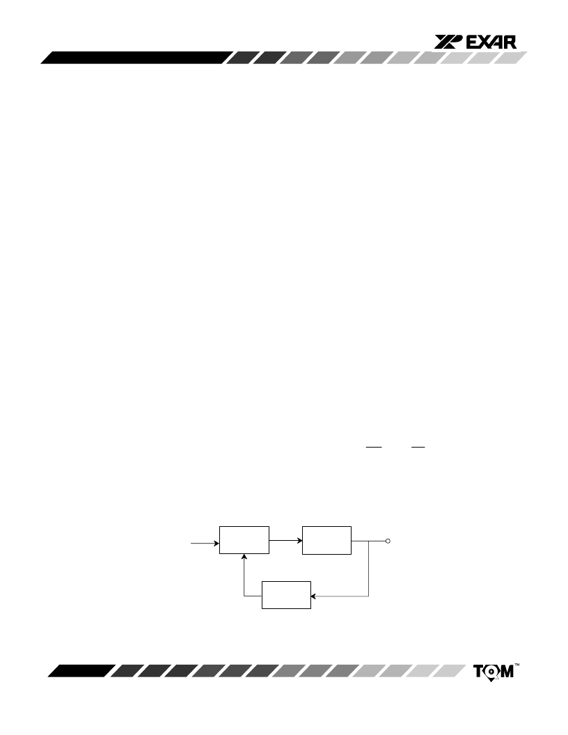
As shown in Figure 13 the PLL is a feedback system
comprised of three basic functional blocks: phase
comparator, low-pass filter and voltage-controlled
oscillator (VCO). The basic principle of operation of a PLL
can be briefly explained as follows: with no input signal
applied to the system, the error voltage V
d
, is equal to
zero. The VCO operates at a set frequency, f
o
, which is
known as the “free-running” frequency. If an input signal is
applied to the system, the phase comparator compares
the phase and frequency of the input signal with the VCO
frequency and generates an error voltage, V
e
(t), that is
related to the phase and frequency difference between
the two signals. This error voltage is then filtered and
applied to the control terminal of the VCO. If the input
frequency, fs, is sufficiently close to f
o
, the feedback
nature of the PLL causes the VCO to synchronize or “l(fā)ock”
with the incoming signal. Once in lock, the VCO frequency
is identical to the input signal, except for a finite phase
difference.
A Linearized Model for PLL
When the PLL is in lock, it can be approximated by the
linear feedback system shown in Figure 14.
s
and
o
are
the respective phase angles associated with the input
signal and the VCO output, F(s) is the low-pass filter
response in frequency domain, and K
d
and K
o
are the
conversion gains associated with the phase comparator
and VCO sections of the PLL.
DEFINITION OF XR-215A PARAMETERS USED FOR
PLL APPLICATIONS DESIGN
VCO Free-Running Frequency, f
o
The VCO frequency with no input signal is determined by
selection of C
0
across pins 13 and 14 and can be
increased by connecting an external resistor R
X
between
pins 9 and 10. It can be approximated as:
f
0
220
C
0
1
0.6
R
X
where C
0
is in F and R
X
is in k . (See Figure 8.)
Figure 13. Block Diagram of a Phase-Locked Loop
f
s
Input
Signal
V
S
(t)
Phase
Comparator
Lowpass
Filter
VCO
V
e
(t)
V
d
(t)
V
d
(t)
f
o
V
O
(t)
相關PDF資料 |
PDF描述 |
|---|---|
| XR-215 | Monolithic Phase Locked Loop |
| XR-2207 | Voltage-Controlled Oscillator |
| XR-2207CP | Voltage-Controlled Oscillator |
| XR-2207D | Voltage-Controlled Oscillator |
| XR-2207M | Voltage-Controlled Oscillator |
相關代理商/技術參數(shù) |
參數(shù)描述 |
|---|---|
| XR-215ACD | 制造商:EXAR 制造商全稱:EXAR 功能描述:Monolithic Phase Locked Loop |
| XR-215ACP | 制造商:EXAR 制造商全稱:EXAR 功能描述:Monolithic Phase Locked Loop |
| XR215CP | 制造商:未知廠家 制造商全稱:未知廠家 功能描述:IC-PHASE LOCKED LOOP |
| XR-215CP | 制造商:未知廠家 制造商全稱:未知廠家 功能描述:Analog Phase-Locked Loop |
| XR-215D | 制造商:未知廠家 制造商全稱:未知廠家 功能描述:Analog Phase-Locked Loop |
發(fā)布緊急采購,3分鐘左右您將得到回復。