- 您現(xiàn)在的位置:買(mǎi)賣IC網(wǎng) > PDF目錄372886 > XCS05XL-3CS208I (Xilinx, Inc.) Spartan and Spartan-XL Families Field Programmable Gate Arrays PDF資料下載
參數(shù)資料
| 型號(hào): | XCS05XL-3CS208I |
| 廠商: | Xilinx, Inc. |
| 英文描述: | Spartan and Spartan-XL Families Field Programmable Gate Arrays |
| 中文描述: | 斯巴達(dá)和Spartan - xL的家庭現(xiàn)場(chǎng)可編程門(mén)陣列 |
| 文件頁(yè)數(shù): | 55/66頁(yè) |
| 文件大小: | 809K |
| 代理商: | XCS05XL-3CS208I |
第1頁(yè)第2頁(yè)第3頁(yè)第4頁(yè)第5頁(yè)第6頁(yè)第7頁(yè)第8頁(yè)第9頁(yè)第10頁(yè)第11頁(yè)第12頁(yè)第13頁(yè)第14頁(yè)第15頁(yè)第16頁(yè)第17頁(yè)第18頁(yè)第19頁(yè)第20頁(yè)第21頁(yè)第22頁(yè)第23頁(yè)第24頁(yè)第25頁(yè)第26頁(yè)第27頁(yè)第28頁(yè)第29頁(yè)第30頁(yè)第31頁(yè)第32頁(yè)第33頁(yè)第34頁(yè)第35頁(yè)第36頁(yè)第37頁(yè)第38頁(yè)第39頁(yè)第40頁(yè)第41頁(yè)第42頁(yè)第43頁(yè)第44頁(yè)第45頁(yè)第46頁(yè)第47頁(yè)第48頁(yè)第49頁(yè)第50頁(yè)第51頁(yè)第52頁(yè)第53頁(yè)第54頁(yè)當(dāng)前第55頁(yè)第56頁(yè)第57頁(yè)第58頁(yè)第59頁(yè)第60頁(yè)第61頁(yè)第62頁(yè)第63頁(yè)第64頁(yè)第65頁(yè)第66頁(yè)
R
DS060 (v1.5) March 2, 2000
Powered by ICminer.com Electronic-Library Service CopyRight 2003
4-55
Spartan and Spartan-XL Families Field Programmable Gate Arrays
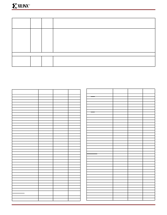
Device-Specific Pinout Tables
Device-specific tables include all packages for each Spartan and Spartan-XL device. They follow the pad locations around
the die, and include boundary scan register locations.
XCS05 & XCS05XL Device Pinouts
DOUT
O
I/O
During Slave Serial or Master Serial configuration, DOUT is the serial configuration data
output that can drive the DIN of daisy-chained slave FPGAs. DOUT data changes on
the falling edge of CCLK, one-and-a-half CCLK periods after it was received at the DIN
input.
In Spartan-XL Express mode, DOUT is the status output that can drive the CS1 of dai-
sy-chained FPGAs, to enable and disable downstream devices.
After configuration, DOUT is a user-programmable I/O pin.
Unrestricted User-Programmable I/O Pins
These pins can be configured to be input and/or output after configuration is completed.
Before configuration is completed, these pins have an internal high-value pull-up resis-
tor network that defines the logic level as High.
I/O
Weak
Pull-up
I/O
Table 18: Pin Descriptions (Continued)
Pin Name
I/O
During
Config.
I/O
After
Config.
Pin Description
XCS05/XL
Pad Name
PC84
VQ100
Bndry Scan
VCC
I/O
I/O
I/O
I/O
I/O
I/O
I/O
I/O
I/O
I/O, SGCK1
, GCK8
VCC
GND
I/O, PGCK1
, GCK1
I/O
I/O, TDI
I/O, TCK
I/O, TMS
I/O
I/O
I/O
I/O
GND
VCC
I/O
I/O
I/O
I/O
I/O
I/O
I/O
I/O
I/O, SGCK2
, GCK2
Not Connected
, M1
GND
MODE
, M0
VCC
Not Connected
,
PWRDWN
I/O, PGCK2
, GCK3
I/O (HDC)
P2
P3
P4
-
-
P5
P6
P7
P8
P9
P10
P11
P12
P13
P14
P15
P16
P17
P18
-
P19
P20
P21
P22
P23
P24
-
P25
P26
P27
-
P28
P29
P30
P31
P32
P33
P34
P89
P90
P91
P92
P93
P94
P95
P96
P97
P98
P99
P100
P1
P2
P3
P4
P5
P6
P7
P8
P9
P10
P11
P12
P13
P14
P15
P16
P17
P18
P19
P20
P21
P22
P23
P24
P25
P26
-
32
35
38
41
44
47
50
53
56
59
-
-
62
65
68
71
74
77
83
86
89
-
-
92
95
98
104
107
110
113
116
119
122
-
125
-
126
P35
P36
P27
P28
127
130
I/O
I/O (LDC)
I/O
I/O
I/O
I/O
I/O
I/O (INIT)
VCC
GND
I/O
I/O
I/O
I/O
I/O
I/O
I/O
I/O
I/O
I/O, SGCK3
, GCK4
GND
DONE
VCC
PROGRAM
I/O (D7
)
I/O, PGCK3
, GCK5
I/O (D6
)
I/O
I/O (D5
)
I/O
I/O
I/O
I/O (D4
)
I/O
VCC
GND
I/O (D3
)
I/O
I/O
I/O (D2
)
I/O
-
P29
P30
P31
P32
P33
P34
P35
P36
P37
P38
P39
P40
P41
P42
P43
P44
P45
P46
P47
P48
P49
P50
P51
P52
P53
P54
P55
P56
P57
P58
P59
P60
P61
P62
P63
P64
P65
P66
P67
P68
P69
133
136
139
142
145
148
151
154
-
-
157
160
163
166
169
172
175
178
181
184
-
-
-
-
187
190
193
196
199
202
205
208
211
214
-
-
217
220
223
229
232
P37
P38
P39
-
-
P40
P41
P42
P43
P44
P45
-
-
P46
P47
P48
P49
P50
P51
P52
P53
P54
P55
P56
P57
P58
-
P59
P60
-
-
P61
P62
P63
P64
P65
P66
-
P67
P68
XCS05/XL
Pad Name
PC84
VQ100
Bndry Scan
相關(guān)PDF資料 |
PDF描述 |
|---|---|
| XCS05XL-3CS240C | Spartan and Spartan-XL Families Field Programmable Gate Arrays |
| XCS05XL-3CS240I | Spartan and Spartan-XL Families Field Programmable Gate Arrays |
| XCS05XL-3CS256C | Spartan and Spartan-XL Families Field Programmable Gate Arrays |
| XCS05XL-3CS256I | Spartan and Spartan-XL Families Field Programmable Gate Arrays |
| XCS05XL-3CS280C | Spartan and Spartan-XL Families Field Programmable Gate Arrays |
相關(guān)代理商/技術(shù)參數(shù) |
參數(shù)描述 |
|---|---|
| XCS05XL-3CS240C | 制造商:XILINX 制造商全稱:XILINX 功能描述:Spartan and Spartan-XL Families Field Programmable Gate Arrays |
| XCS05XL-3CS240I | 制造商:XILINX 制造商全稱:XILINX 功能描述:Spartan and Spartan-XL Families Field Programmable Gate Arrays |
| XCS05XL-3CS256C | 制造商:XILINX 制造商全稱:XILINX 功能描述:Spartan and Spartan-XL Families Field Programmable Gate Arrays |
| XCS05XL-3CS256I | 制造商:XILINX 制造商全稱:XILINX 功能描述:Spartan and Spartan-XL Families Field Programmable Gate Arrays |
| XCS05XL-3CS280C | 制造商:XILINX 制造商全稱:XILINX 功能描述:Spartan and Spartan-XL Families Field Programmable Gate Arrays |
發(fā)布緊急采購(gòu),3分鐘左右您將得到回復(fù)。