- 您現(xiàn)在的位置:買賣IC網(wǎng) > PDF目錄19467 > XCR3256XL-7PQ208C (Xilinx Inc)IC CPLD 256MCELL 3.3V HP 208PQFP PDF資料下載
參數(shù)資料
| 型號: | XCR3256XL-7PQ208C |
| 廠商: | Xilinx Inc |
| 文件頁數(shù): | 8/12頁 |
| 文件大小: | 0K |
| 描述: | IC CPLD 256MCELL 3.3V HP 208PQFP |
| 標(biāo)準(zhǔn)包裝: | 24 |
| 系列: | CoolRunner XPLA3 |
| 可編程類型: | 系統(tǒng)內(nèi)可編程(最少 1K 次編程/擦除循環(huán)) |
| 最大延遲時間 tpd(1): | 7.0ns |
| 電壓電源 - 內(nèi)部: | 3 V ~ 3.6 V |
| 邏輯元件/邏輯塊數(shù)目: | 16 |
| 宏單元數(shù): | 256 |
| 門數(shù): | 6000 |
| 輸入/輸出數(shù): | 164 |
| 工作溫度: | 0°C ~ 70°C |
| 安裝類型: | 表面貼裝 |
| 封裝/外殼: | 208-BFQFP |
| 供應(yīng)商設(shè)備封裝: | 208-PQFP(28x28) |
| 包裝: | 托盤 |

CoolRunner XPLA3 CPLD
DS012 (v2.5) May 26, 2009
Product Specification
R
mented in the buried macrocell can be fed back to the ZIA
via the macrocell feedback path.
If a macrocell pin is configured as a registered input, there is
a direct path to the register to provide a fast input setup
time. If the macrocell is configured as a latch, the register
clock input functions as the latch enable, with the latch
transparent when this signal is High. The hardwired clock
enable is non-functional when the macrocell is configured
as a latch.
I/O Cell
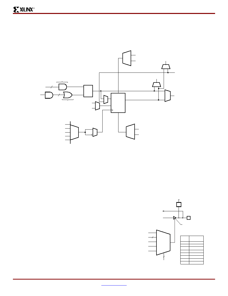
The OE (Output Enable) multiplexer has eight possible
modes (Figure 6). When the I/O Cell is configured as an
input (or 3-stated output), a half latch feature exists. This
half latch pulls the input High (through a weak pull-up) if the
input should float and cross the threshold. This protects the
input from staying in the linear region and causing an
increased amount of power consumption. This same weak
pull-up can be enabled in software such that it is always on
when the I/O Cell is configured as an input. This weak pull
up is automatically turned on when a pin is unused by the
design.
The I/O Cell is 5V tolerant when the device is powered.
Each output has independent slew rate control (fast or slow)
which assists in reducing EMI emissions.
See individual device data sheets for 3.3V PCI electrical
specification compatibility.
Note that an I/O macrocell used as buried logic that does
not have the I/O pin used for input is considered to be
unused, and the weak pull-up resistors will be turned on. It
is recommended that any unused I/O pins on the CoolRun-
ner XPLA3 family of CPLDs be left unconnected. Dedicated
input pins (CLKx/INx) do not have on-chip weak pull-up
resistors; therefore unused dedicated input pins must have
external termination. As with all CMOS devices, do not
allow inputs to float.
Figure 5: XPLA3 Macrocell Architecture
Global CLK
Universal CLK
P-term CLK
CT [4:7]
ds012_05_122299
Universal PST
CT [0:5]
Universal RST
CT [0:5]
To ZIA
To I/O
PAD
Note: Global CLK signals come from pins.
To ZIA
VFM
RST
PST
D/T/L
CLKEn
Q
CT4
P-term
48
PLA OR Term
From PT Array
1
Figure 6: I/O Cell
GND (Weak P.U.)
VCC
Universal OE
CT
GND
OE [2:0]
To Macrocell / ZIA
From Macrocell
I/O Pin
WP
Slew
Control
OE
Decode
0
1
2
3
4
5
6
7
I/O Pin
State
3-State
Function CT0
Function CT1
Function CT2
Function CT6
Universal OE
Enable
Weak P.U.
ds012_06_121699
Weak Pull-up
OE = 7
VCC
3
4
相關(guān)PDF資料 |
PDF描述 |
|---|---|
| GCC05DREN | CONN EDGECARD 10POS .100 EYELET |
| VE-21J-CY-F4 | CONVERTER MOD DC/DC 36V 50W |
| VE-B12-CX-B1 | CONVERTER MOD DC/DC 15V 75W |
| VE-B70-CY-F2 | CONVERTER MOD DC/DC 5V 50W |
| ADSP-21369BBPZ-2A | IC DSP 32BIT 333MHZ 256-BGA |
相關(guān)代理商/技術(shù)參數(shù) |
參數(shù)描述 |
|---|---|
| XCR3256XL-7PQ208I | 制造商:XILINX 制造商全稱:XILINX 功能描述:256 Macrocell CPLD |
| XCR3256XL-7PQ256C | 制造商:XILINX 制造商全稱:XILINX 功能描述:256 Macrocell CPLD |
| XCR3256XL-7PQ256I | 制造商:XILINX 制造商全稱:XILINX 功能描述:256 Macrocell CPLD |
| XCR3256XL-7PQ280C | 制造商:XILINX 制造商全稱:XILINX 功能描述:256 Macrocell CPLD |
| XCR3256XL-7PQ280I | 制造商:XILINX 制造商全稱:XILINX 功能描述:256 Macrocell CPLD |
發(fā)布緊急采購,3分鐘左右您將得到回復(fù)。