- 您現(xiàn)在的位置:買賣IC網(wǎng) > PDF目錄225573 > XC7K420T-3FFG901I (XILINX INC) FPGA, PBGA900 PDF資料下載
參數(shù)資料
| 型號(hào): | XC7K420T-3FFG901I |
| 廠商: | XILINX INC |
| 元件分類: | FPGA |
| 英文描述: | FPGA, PBGA900 |
| 封裝: | LEAD FREE, FBGA-900 |
| 文件頁數(shù): | 34/50頁 |
| 文件大小: | 1218K |
| 代理商: | XC7K420T-3FFG901I |
第1頁第2頁第3頁第4頁第5頁第6頁第7頁第8頁第9頁第10頁第11頁第12頁第13頁第14頁第15頁第16頁第17頁第18頁第19頁第20頁第21頁第22頁第23頁第24頁第25頁第26頁第27頁第28頁第29頁第30頁第31頁第32頁第33頁當(dāng)前第34頁第35頁第36頁第37頁第38頁第39頁第40頁第41頁第42頁第43頁第44頁第45頁第46頁第47頁第48頁第49頁第50頁
Kintex-7 FPGAs Data Sheet: DC and Switching Characteristics
DS182 (v1.1) April 1, 2011
Advance Product Specification
4
Power-On/Off Power Supply Requirements
Xilinx FPGAs require a certain amount of supply current during power-on to insure proper device initialization. The actual
current consumed depends on the power-on ramp rate of the power supply.
The recommended power-on and reverse power-off sequence for Kintex-7 devices is VCCINT, VCCBRAM, VCCAUX, VCCAUX_IO,
and VCCO to achieve minimum current draw and ensure I/Os are 3-stated at power-up. In cases where the recommended
sequence cannot be met, the following rules ensure that the I/Os remain 3-stated and no device damage will occur. VCCINT
and VCCBRAM can be powered on or off at any time as long as the following rules are met:
VCCAUX and VCCAUX_IO must be powered prior to VCCO or VCCAUX, VCCAUX_IO, and VCCO can ramp simultaneously if
powered by the same supply.
VCCAUX and VCCO can be powered by the same supply.
During operation, the VCCAUX,VCCAUX_IO, and VCCINT voltages must stay within their specifications (see Table 2).
When powering down, the reverse power-up sequencing rules are recommended for the same reasons given during power
up. VCCO must be powered down prior to VCCAUX and VCCAUX_IO, or if powered by the same supply, VCCO can be powered
down simultaneously.
In -3, -2, and -1 devices, if VCCINT and VCCBRAM have the same recommended voltage levels, then both can be powered by
the same supply. Both VCCINT and VCCBRAM can be powered up or down any time during the recommended sequence.
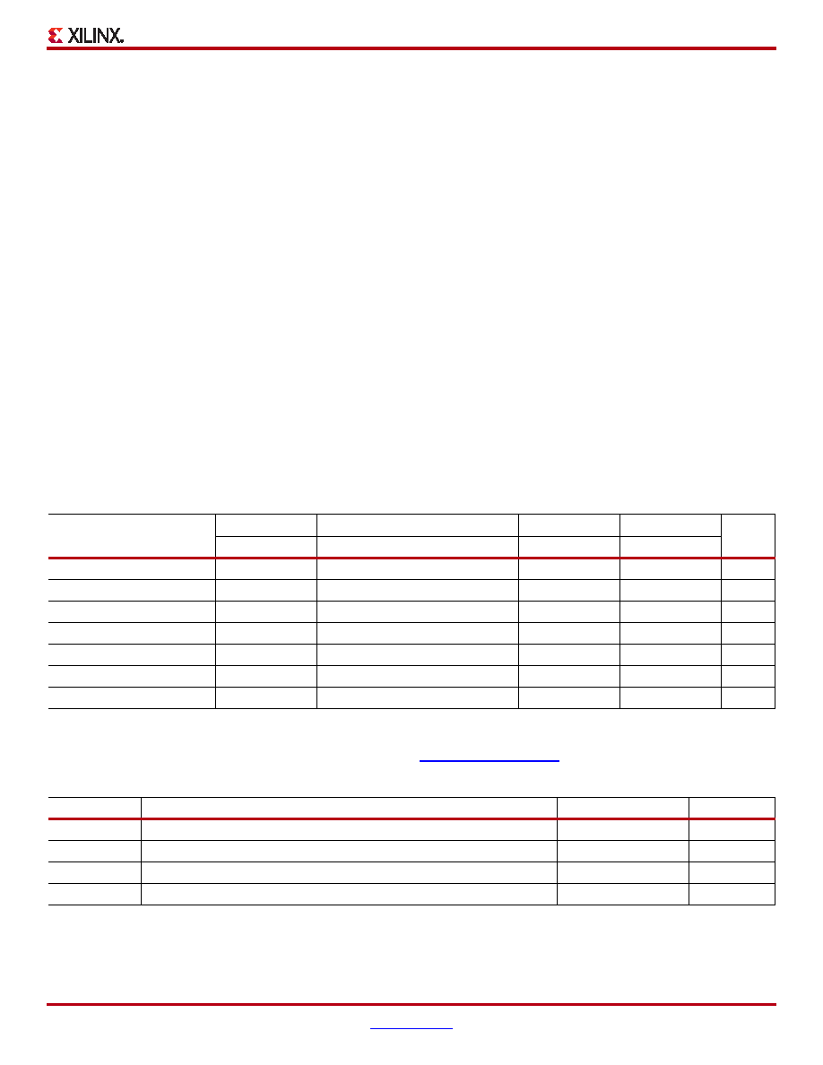
Table 5 shows the minimum current, in addition to ICCQ, that are required by Kintex-7 devices for proper power-on and
configuration. If the current minimums shown in Table 4 and Table 5 are met, the device powers on after all three supplies
have passed through their power-on reset threshold voltages. The FPGA must not be configured until after VCCINT is
applied.
Once initialized and configured, use the XPOWER tools to estimate current drain on these supplies.
Table 5: Power-On Current for Kintex-7 Devices
Device
ICCINTMIN
ICCAUXMIN
ICCOMIN
ICCAUX_IO
ICCBRAM
Units
Typ(1)
Typ(1)
XC7K70T
mA
XC7K160T
mA
XC7K325T
mA
XC7K355T
mA
XC7K410T
mA
XC7K420T
mA
XC7K480T
mA
Notes:
1.
Typical values are specified at nominal voltage, 25°C.
2.
Use the XPOWER Estimator (XPE) spreadsheet tool (download at http://www.xilinx.com/power) to calculate maximum power-on currents.
Table 6: Power Supply Ramp Time
Symbol
Description
Ramp Time
Units
VCCINT
Internal supply voltage relative to GND
0.20 to 50.0
ms
VCCO
Output drivers supply voltage relative to GND
0.20 to 50.0
ms
VCCAUX
Auxiliary supply voltage relative to GND
0.20 to 50.0
ms
VCCBRAM
Block RAM supply voltage relative to GND
0.20 to 50.0
ms
相關(guān)PDF資料 |
PDF描述 |
|---|---|
| XC8106-ESPC84C | FPGA, 1728 CLBS, 5616 GATES, PQCC84 |
| XC8106-ESPC84I | FPGA, 1728 CLBS, 5616 GATES, PQCC84 |
| XC8106-ESPQ100C | FPGA, 1728 CLBS, 5616 GATES, PQFP100 |
| XC8106-ESPQ100I | FPGA, 1728 CLBS, 5616 GATES, PQFP100 |
| XC8106-ESPQ160C | FPGA, 1728 CLBS, 5616 GATES, PQFP160 |
相關(guān)代理商/技術(shù)參數(shù) |
參數(shù)描述 |
|---|---|
| XC7K420T-L2FF1156E | 制造商:Xilinx 功能描述:KINTEX-7 - Trays 制造商:Xilinx 功能描述:IC FPGA 400 I/O 1156FCBGA |
| XC7K420T-L2FF901E | 制造商:Xilinx 功能描述:KINTEX-7 - Trays 制造商:Xilinx 功能描述:IC FPGA 420K KINTEX-7 901FBGA 制造商:Xilinx 功能描述:IC FPGA 380 I/O 901FCBGA |
| XC7K420T-L2FFG1156E | 制造商:Xilinx 功能描述:KINTEX-7 - Trays 制造商:Xilinx 功能描述:IC FPGA 400 I/O 1156FCBGA |
| XC7K420T-L2FFG901E | 制造商:Xilinx 功能描述:KINTEX-7 - Trays 制造商:Xilinx 功能描述:IC FPGA 380 I/O 901FCBGA |
| XC7K480T-1FF1156C | 制造商:Xilinx 功能描述:KINTEX-7 - Trays 制造商:Xilinx 功能描述:IC FPGA 400 I/O 1156FCBGA |
發(fā)布緊急采購,3分鐘左右您將得到回復(fù)。