- 您現(xiàn)在的位置:買賣IC網(wǎng) > PDF目錄1973 > XC5202-5PQ100C (Xilinx Inc)IC - FPGA SPEED GRADE 5 COM TEMP PDF資料下載
參數(shù)資料
| 型號: | XC5202-5PQ100C |
| 廠商: | Xilinx Inc |
| 文件頁數(shù): | 27/73頁 |
| 文件大?。?/td> | 0K |
| 描述: | IC - FPGA SPEED GRADE 5 COM TEMP |
| 產(chǎn)品變化通告: | XC1700 PROMs,XC5200,HQ,SCD Parts Discontinuation 19/Jul/2010 |
| 標(biāo)準(zhǔn)包裝: | 66 |
| 系列: | XC5200 |
| LAB/CLB數(shù): | 64 |
| 邏輯元件/單元數(shù): | 256 |
| 輸入/輸出數(shù): | 81 |
| 門數(shù): | 3000 |
| 電源電壓: | 4.75 V ~ 5.25 V |
| 安裝類型: | 表面貼裝 |
| 工作溫度: | 0°C ~ 85°C |
| 封裝/外殼: | 100-BQFP |
| 供應(yīng)商設(shè)備封裝: | 100-QFP(14x20) |
| 其它名稱: | Q858790 XC5202-5PQ1000C XC5202-5PQ1000C-ND |
第1頁第2頁第3頁第4頁第5頁第6頁第7頁第8頁第9頁第10頁第11頁第12頁第13頁第14頁第15頁第16頁第17頁第18頁第19頁第20頁第21頁第22頁第23頁第24頁第25頁第26頁當(dāng)前第27頁第28頁第29頁第30頁第31頁第32頁第33頁第34頁第35頁第36頁第37頁第38頁第39頁第40頁第41頁第42頁第43頁第44頁第45頁第46頁第47頁第48頁第49頁第50頁第51頁第52頁第53頁第54頁第55頁第56頁第57頁第58頁第59頁第60頁第61頁第62頁第63頁第64頁第65頁第66頁第67頁第68頁第69頁第70頁第71頁第72頁第73頁

R
November 5, 1998 (Version 5.2)
7-115
XC5200 Series Field Programmable Gate Arrays
7
Master Serial Mode
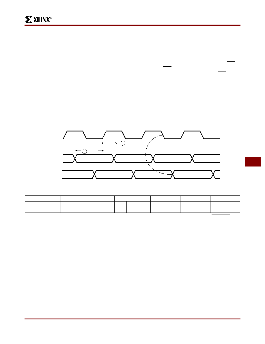
In Master Serial mode, the CCLK output of the lead FPGA
drives a Xilinx Serial PROM that feeds the FPGA DIN input.
Each rising edge of the CCLK output increments the Serial
PROM internal address counter. The next data bit is put on
the SPROM data output, connected to the FPGA DIN pin.
The lead FPGA accepts this data on the subsequent rising
CCLK edge.
The lead FPGA then presents the preamble data—and all
data that overflows the lead device—on its DOUT pin.
There is an internal pipeline delay of 1.5 CCLK periods,
which means that DOUT changes on the falling CCLK
edge, and the next FPGA in the daisy chain accepts data
on the subsequent rising CCLK edge.
In the bitstream generation software, the user can specify
Fast ConfigRate, which, starting several bits into the first
frame, increases the CCLK frequency by a factor of twelve.
The value increases from a nominal 1 MHz, to a nominal 12
MHz. Be sure that the serial PROM and slaves are fast
enough to support this data rate. The Medium ConfigRate
option changes the frequency to a nominal 6 MHz.
XC2000, XC3000/A, and XC3100A devices do not support
the Fast or Medium ConfigRate options.
The SPROM CE input can be driven from either LDC or
DONE. Using LDC avoids potential contention on the DIN
pin, if this pin is configured as user-I/O, but LDC is then
restricted to be a permanently High user output after con-
figuration. Using DONE can also avoid contention on DIN,
provided the DONE before I/O enable option is invoked.
Figure 28 on page 114 shows a full master/slave system.
The leftmost device is in Master Serial mode.
Master Serial mode is selected by a <000> on the mode
pins (M2, M1, M0).
Notes:
1. At power-up, Vcc must rise from 2.0 V to Vcc min in less than 25 ms, otherwise delay configuration by pulling PROGRAM
Low until Vcc is valid.
2. Master Serial mode timing is based on testing in slave mode.
Figure 30: Master Serial Mode Programming Switching Characteristics
In the two Master Parallel modes, the lead FPGA directly
addresses an industry-standard byte-wide EPROM, and
accepts eight data bits just before incrementing or decre-
menting the address outputs.
The eight data bits are serialized in the lead FPGA, which
then presents the preamble data—and all data that over-
flows the lead device—on its DOUT pin. There is an inter-
nal delay of 1.5 CCLK periods, after the rising CCLK edge
that accepts a byte of data (and also changes the EPROM
address) until the falling CCLK edge that makes the LSB
(D0) of this byte appear at DOUT. This means that DOUT
changes on the falling CCLK edge, and the next FPGA in
the daisy chain accepts data on the subsequent rising
CCLK edge.
The PROM address pins can be incremented or decre-
mented, depending on the mode pin settings. This option
allows the FPGA to share the PROM with a wide variety of
microprocessors and microcontrollers. Some processors
must boot from the bottom of memory (all zeros) while oth-
ers must boot from the top. The FPGA is flexible and can
load its configuration bitstream from either end of the mem-
ory.
Master Parallel Up mode is selected by a <100> on the
mode pins (M2, M1, M0). The EPROM addresses start at
00000 and increment.
Master Parallel Down mode is selected by a <110> on the
mode pins. The EPROM addresses start at 3FFFF and
decrement.
Serial Data In
CCLK
(Output)
Serial DOUT
(Output)
1
TDSCK
2
TCKDS
n
n + 1
n + 2
n – 3
n – 2
n – 1
n
X3223
Description
Symbol
Min
Max
Units
CCLK
DIN setup
1
TDSCK
20
ns
DIN hold
2
TCKDS
0ns
Product Obsolete or Under Obsolescence
相關(guān)PDF資料 |
PDF描述 |
|---|---|
| XC56309AG100AR2 | IC DSP 24BIT 100MHZ 144-LQFP |
| XC56L307VF160 | IC DSP 24BIT FIXED POINT 196-BGA |
| XC56L307VL160 | IC DSP 24BIT FIXED POINT 196-BGA |
| XC5VLX220T-1FFG1136I | IC FPGA VIRTEX-5 220K 1136FBGA |
| XC5VSX35T-X1FFG665C | IC FPGA VIRTEX 5 35K 665FFGBGA |
相關(guān)代理商/技術(shù)參數(shù) |
參數(shù)描述 |
|---|---|
| XC5202-5PQ100I | 制造商:未知廠家 制造商全稱:未知廠家 功能描述:Field Programmable Gate Array (FPGA) |
| XC5202-5PQ160C | 制造商:XILINX 制造商全稱:XILINX 功能描述:Field Programmable Gate Arrays |
| XC5202-5PQ208C | 制造商:XILINX 制造商全稱:XILINX 功能描述:Field Programmable Gate Arrays |
| XC5202-5PQ240C | 制造商:XILINX 制造商全稱:XILINX 功能描述:Field Programmable Gate Arrays |
| XC5202-5TQ144C | 制造商:XILINX 制造商全稱:XILINX 功能描述:Field Programmable Gate Arrays |
發(fā)布緊急采購,3分鐘左右您將得到回復(fù)。