- 您現(xiàn)在的位置:買賣IC網(wǎng) > PDF目錄225572 > XC4VFX100-11FF1152I (XILINX INC) FPGA, 10544 CLBS, 1181 MHz, PBGA1152 PDF資料下載
參數(shù)資料
| 型號: | XC4VFX100-11FF1152I |
| 廠商: | XILINX INC |
| 元件分類: | FPGA |
| 英文描述: | FPGA, 10544 CLBS, 1181 MHz, PBGA1152 |
| 封裝: | FBGA-1152 |
| 文件頁數(shù): | 7/58頁 |
| 文件大小: | 1863K |
| 代理商: | XC4VFX100-11FF1152I |
第1頁第2頁第3頁第4頁第5頁第6頁當(dāng)前第7頁第8頁第9頁第10頁第11頁第12頁第13頁第14頁第15頁第16頁第17頁第18頁第19頁第20頁第21頁第22頁第23頁第24頁第25頁第26頁第27頁第28頁第29頁第30頁第31頁第32頁第33頁第34頁第35頁第36頁第37頁第38頁第39頁第40頁第41頁第42頁第43頁第44頁第45頁第46頁第47頁第48頁第49頁第50頁第51頁第52頁第53頁第54頁第55頁第56頁第57頁第58頁
Virtex-4 FPGA Data Sheet: DC and Switching Characteristics
DS302 (v3.7) September 9, 2009
Product Specification
15
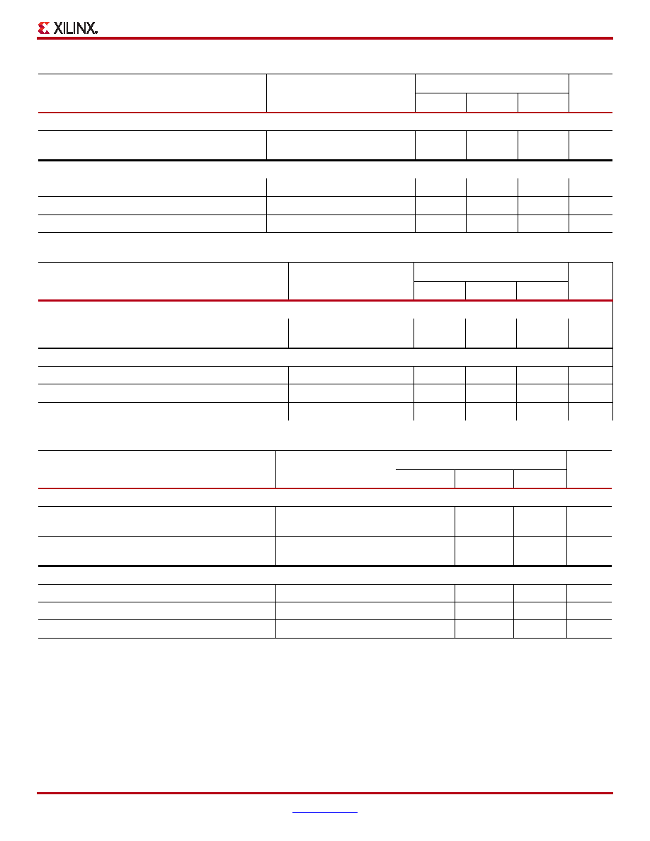
Table 19: PowerPC 405 Data-Side On-Chip Memory Switching Characteristics
Description
Symbol
Speed Grade
Units
-12
-11
-10
Setup and Hold Relative to Clock (BRAMDSOCMCLK)
Data-Side On-Chip Memory data bus inputs
TPPCDCK_DSOCMRDDB
TPPCCKD_DSOCMRDDB
0.60
0.20
0.65
0.20
0.74
0.23
ns, Min
Clock to Out
Data-Side On-Chip Memory control outputs
TPPCCKO_BRAMBWR
2.07
2.30
2.65
ns, Max
Data-Side On-Chip Memory address bus outputs
TPPCCKO_BRAMABUS
2.07
2.30
2.65
ns, Max
Data-Side On-Chip Memory data bus outputs
TPPCCKO_IBRAMWRDBUS01
1.61
1.79
2.06
ns, Max
Table 20: PowerPC 405 Instruction-Side On-Chip Memory Switching Characteristics
Description
Symbol
Speed Grade
Units
-12
-11
-10
Setup and Hold Relative to Clock (BRAMISOCMCLK)
Instruction-Side On-Chip Memory data bus inputs
TPPCDCK_ISOCMRDDB
TPPCCKD_ISOCMRDDB
0.74
0.20
0.82
0.20
0.94
0.23
ns, Min
Clock to Out
Instruction-Side On-Chip Memory control outputs
TPPCCKO_IBRAMEN
3.04
3.37
3.88
ns, Max
Instruction-Side On-Chip Memory address bus outputs
TPPCCKO_IBRAMRDABUS
1.67
1.85
2.13
ns, Max
Instruction-Side On-Chip Memory data bus outputs
TPPCCKO_IBRAMWRDBUS
1.67
1.86
2.14
ns, Max
Table 21: Processor Block DCR Bus Switching Characteristics
Description
Symbol
Speed Grade
Units
-12
-11
-10
Setup and Hold Relative to Clock (CPMDCRCLOCK)
Device Control Register Bus control inputs
TPPCDCK_EXDCRACK
TPPCCKD_EXDCRACK
0.12
0.15
0.13
0.17
0.15
0.19
ns, Min
Device Control Register Bus data inputs
TPPCDCK_EXDCRDBUSI
TPPCCKD_EXDCRDBUSI
0.57
0.16
0.57
0.16
1.02
0.27
ns, Min
Clock to Out
Device Control Register Bus control outputs
TPPCCKO_EXDCRRD
1.20
1.35
1.54
ns, Max
Device Control Register Bus address bus outputs
TPPCCKO_EXDCRABUS
1.28
1.45
1.66
ns, Max
Device Control Register Bus data bus outputs
TPPCCKO_EXDCRDBUSO
1.31
1.45
1.67
ns, Max
相關(guān)PDF資料 |
PDF描述 |
|---|---|
| XC4VFX100-11FF1517I | FPGA, 10544 CLBS, 1181 MHz, PBGA1517 |
| XC4VFX100-10FFG1152I | FPGA, 10544 CLBS, 1028 MHz, PBGA1152 |
| XC4VFX100-10FFG1517I | FPGA, 10544 CLBS, 1028 MHz, PBGA1517 |
| XC4VFX100-11FFG1152I | FPGA, 10544 CLBS, 1181 MHz, PBGA1152 |
| XC4VFX100-11FFG1517I | FPGA, 10544 CLBS, 1181 MHz, PBGA1517 |
相關(guān)代理商/技術(shù)參數(shù) |
參數(shù)描述 |
|---|---|
| XC4VFX100-11FF1517C | 制造商:Xilinx 功能描述:FPGA VIRTEX-4 94896 CELLS 90NM 1.2V 1517FCBGA - Trays |
| XC4VFX100-11FF1517CES4 | 制造商:Xilinx 功能描述: |
| XC4VFX100-11FF1517CES4S | 制造商:Xilinx 功能描述: |
| XC4VFX100-11FF1517I | 功能描述:IC FPGA VIRTEX-4FX 1517FFBGA RoHS:否 類別:集成電路 (IC) >> 嵌入式 - FPGA(現(xiàn)場可編程門陣列) 系列:Virtex®-4 FX 產(chǎn)品變化通告:XC4000(E,L) Discontinuation 01/April/2002 標(biāo)準(zhǔn)包裝:24 系列:XC4000E/X LAB/CLB數(shù):100 邏輯元件/單元數(shù):238 RAM 位總計:3200 輸入/輸出數(shù):80 門數(shù):3000 電源電壓:4.5 V ~ 5.5 V 安裝類型:表面貼裝 工作溫度:-40°C ~ 100°C 封裝/外殼:120-BCBGA 供應(yīng)商設(shè)備封裝:120-CPGA(34.55x34.55) |
| XC4VFX100-11FF1517IES4 | 制造商:Xilinx 功能描述: |
發(fā)布緊急采購,3分鐘左右您將得到回復(fù)。